
Display panel, display device and electronic equipment

A display panel and substrate technology, which is applied in the direction of identification devices, instruments, etc., can solve the problem of increasing the overall thickness of the display screen

Pending Publication Date: 2020-05-19
BOE TECH GRP CO LTD +1
View PDF10 Cites 0 Cited by
  • Summary
  • Abstract
  • Description
  • Claims
  • Application Information

AI Technical Summary

Problems solved by technology

[0005] In view of this, the embodiments of the present invention provide a display panel, a display device, and electronic equipment, the main purpose of which is to solve the problem of increasing the overall thickness of the display screen by introducing a film with a pressure sensing array in order to realize pressure measurement and control in the traditional micro-LED display screen

Method used


Image

  • Display panel, display device and electronic equipment
  • Display panel, display device and electronic equipment
  • Display panel, display device and electronic equipment

Examples


Embodiment 1

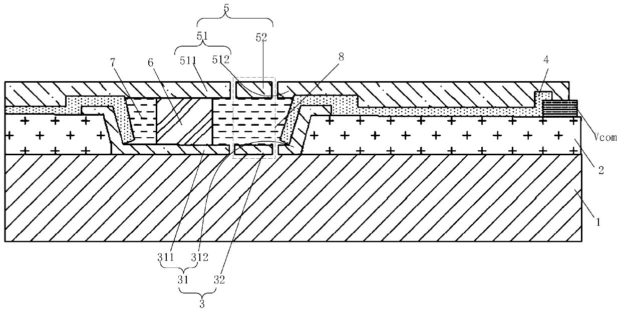
[0043] Further, refer to the attached Figure 1-5 , an embodiment of the present invention provides a display panel. In a specific implementation, the first area 31 includes a first sub-area 311 and a second sub-area 312, and the first sub-area 311 and the second sub-area The regions 312 are arranged at intervals, and the second region 32 is arranged between the first subregion 311 and the second subregion 312 .

[0044] Specifically, on the premise that the second area 32 is adjacent to the first area 31, in the technical solution adopted by the present invention, refer to the attached figure 1 , divide the first area 31 into the first sub-area 311 and the second sub-area 312, and the second area 32 is set in the first sub-area 311 and the second sub-area 312, and the second area 32 is isolated from the first sub-area 311 and the second sub-area 312; correspondingly, the third area 51 also includes the fourth sub-area 511 and the second sub-area 511 Five sub-regions 512, th...

Embodiment 2

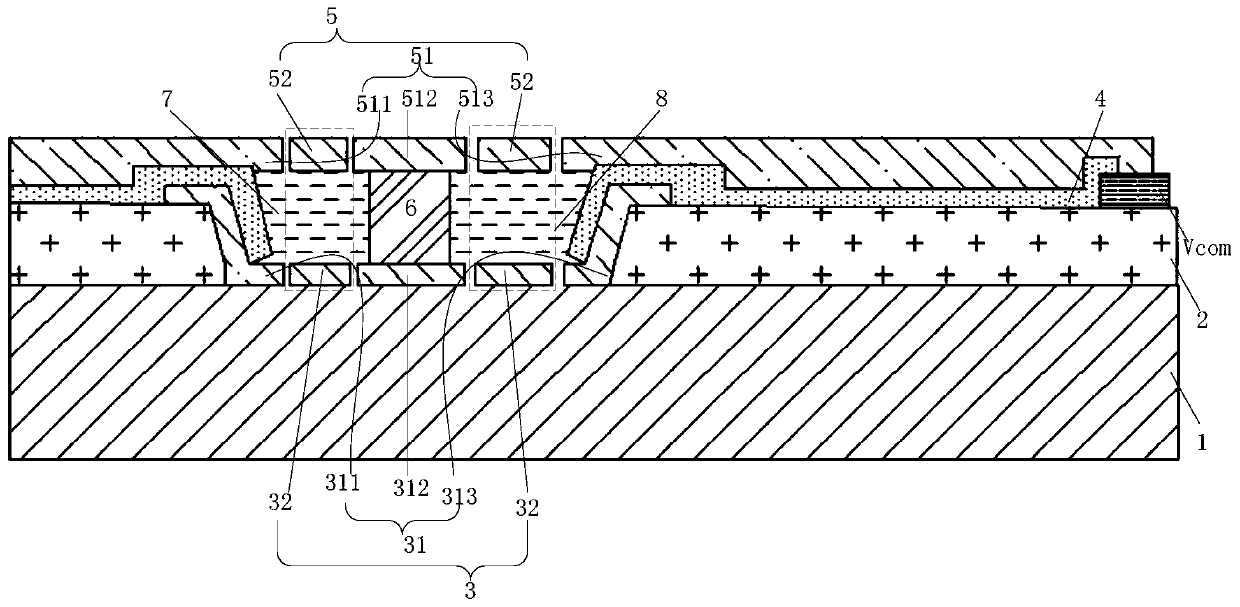
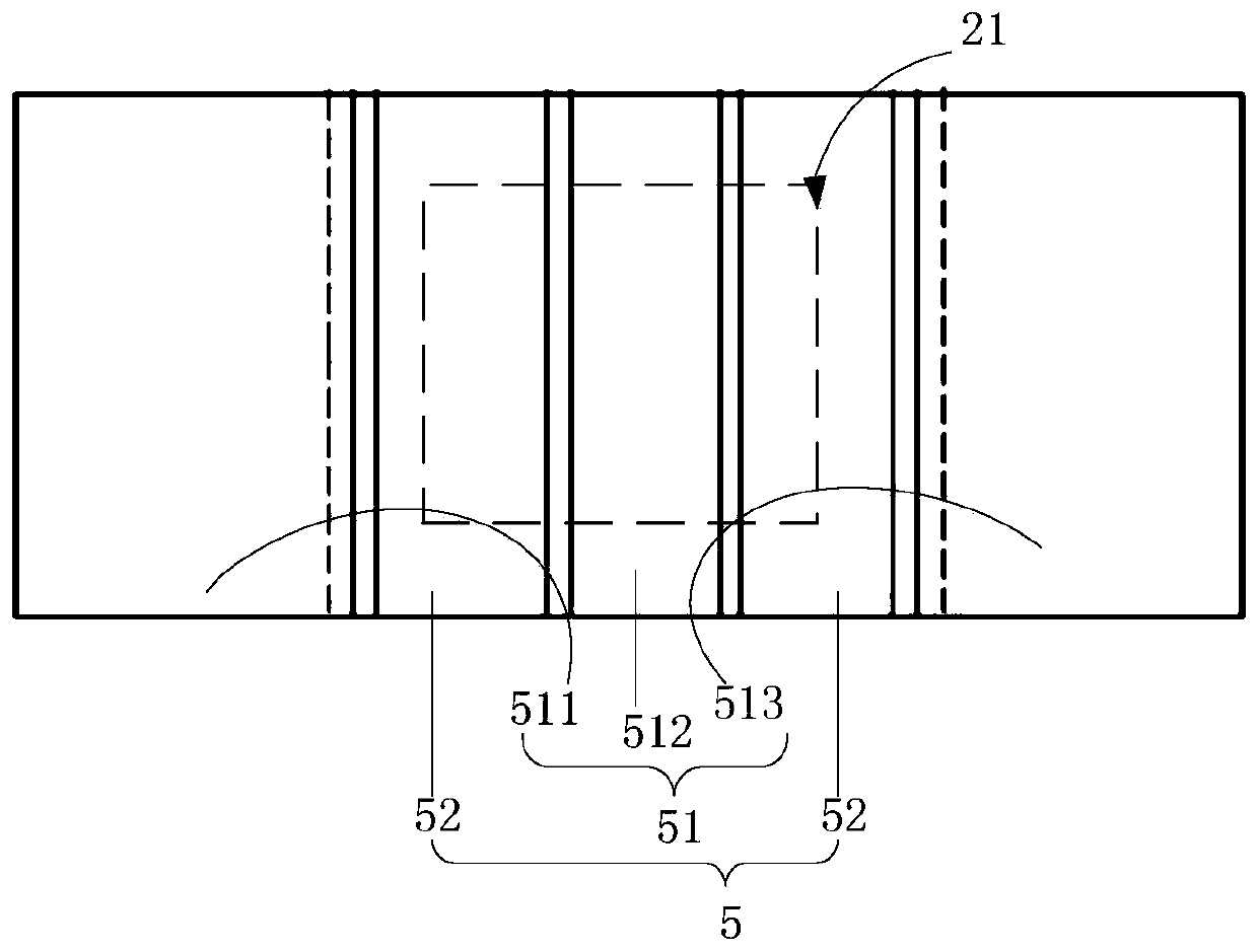
[0047] Further, refer to the attached image 3 And attached figure 2 An embodiment of the present invention provides a display panel. In a specific implementation, the first area 31 includes a first sub-area 311, a second sub-area 312, and a third sub-area 313. The first sub-area 311 The second region 312 is respectively provided between the second subregion 312 and between the second subregion 312 and the third subregion 313 .

[0048] Specifically, on the premise that the third area 51 is adjacent to the first area 31, in the technical solution adopted by the present invention, the first area 31 is partitioned into three-stage first sub-areas 311 , the second sub-area 312 and the third sub-area 313, the second area 32 is arranged between every two sections; correspondingly, the third area 51 is correspondingly cut off into a three-stage fourth sub-area The area 511, the fifth sub-area 512 and the sixth sub-area 513, the fourth sub-area 511, the fifth sub-area 512 and the ...

Embodiment 3

[0055] Further, an embodiment of the present invention provides a display device, which in a specific implementation includes any one of the display panels in the above embodiments or a display panel obtained by combining the above embodiments with each other.

[0056] Specifically, the display device must have a control chip, so the specific working principles of display driving and pressure touch of the display device refer to the content of the above-mentioned embodiments, which will not be repeated here.

[0057] It should be noted that the display panel in this embodiment is the display panel described in any one of the embodiments 1-2 or a display panel obtained by combining each other; and the above is only a preferred embodiment of the present invention. The present invention is not limited in any form, so the above embodiments can be combined, and any simple modifications, equivalent changes and modifications made to the above embodiments according to the technical ess...


PUM


Abstract

The invention discloses a display panel, a display device and electronic equipment. According to the main technical scheme, the display panel comprises a TFT substrate, a black matrix layer, an insulating layer, a second electrode layer and a packaging layer which are sequentially arranged in a stacked mode. The black matrix layer comprises a pixel opening area covered with a first electrode layer; and the position, corresponding to the side wall of the pixel opening area, of the first electrode layer and the black matrix layer are covered with the insulating layer. The first electrode layer comprises a first area and a second area which are separated from each other; the second electrode layer comprises a third area and a fourth area which are separated from each other; the orthographic projection of the first area facing the TFT substrate is in the orthographic projection of the third area facing the TFT substrate, and the orthographic projection of the second area and the orthographic projection of the fourth area facing the TFT substrate are completely overlapped; the light-emitting pixel layer is arranged between the first area and the third area; a passivation layer is arranged between the second area and the fourth area; the capacitance between the second area and the fourth area is changed by the deformation of the passivation layer under the action of an external force.

Description

technical field [0001] The invention relates to the technical field of liquid crystal display, in particular to a display panel, a display device and electronic equipment. Background technique [0002] Micro LED is a new generation of display technology. The LED structure design is thinned, miniaturized, and arrayed. On the circuit substrate; then use the physical deposition process to complete the protective layer and the upper electrode, and then package it to make a Micro LED display substrate. [0003] At present, there are two main trends in the development of micro-LED displays, indoor / outdoor displays with small spacing, large size and high resolution, and wearable devices (such as Apple Watch). The display part of such devices requires high resolution and portable Strong performance, low power consumption and high brightness; adding pressure sensing technology to the micro-LED display for pressure touch detection has become the current development trend; the usual t...

Claims


Application Information

Patent Timeline
IPC IPC(8): G09F9/33
CPCG09F9/33
Inventor 徐佳伟李杨阳范文金
Owner BOE TECH GRP CO LTD
Learn More