Method for manufacturing LCD screen frame decoration piece
A technology for LCD screens and decorative parts, applied in the field of preparation of LCD screen frame decorative parts, can solve problems such as poor apparent flatness, environmental pollution, high mold costs, etc., achieve high apparent texture accuracy, simple transfer printing process, Make reasonable effects
- Summary
- Abstract
- Description
- Claims
- Application Information
AI Technical Summary
Problems solved by technology
Method used
Image

Examples
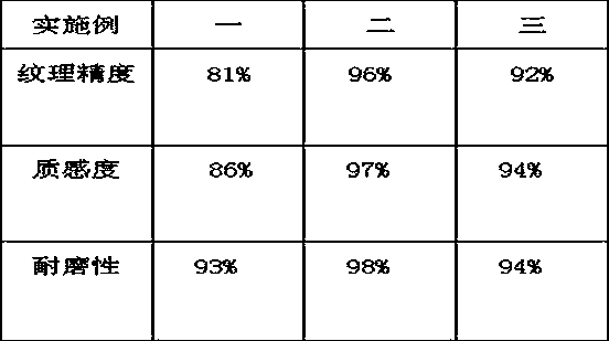
Embodiment 1
[0025] refer to Figure 1-2 , the present embodiment proposes a method for preparing an LCD screen frame decoration, comprising the following steps:
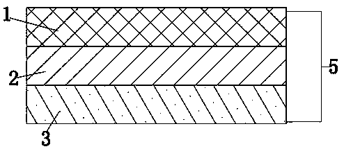
[0026] S1: Take the UV mold and place it on the workbench, and take the raw materials and place them on the side of the UV mold for later use. The raw materials are substrate layer 2 raw material PC transparent sheet and UV resin embossing layer 1 raw material polyurethane acrylic resin;
[0027] S2: Place the PC transparent sheet as the raw material of the substrate layer 2 described in S1 and the polyurethane acrylic resin, the raw material of the UV resin embossing layer 1, in the UV mold from top to bottom, and the thickness of the substrate layer 2 is 0.2mm;
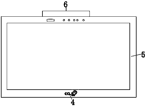
[0028] S3: UV resin embossing layer 1 and substrate layer 2 in S2 are embossed by UV embossing process for 1 minute to obtain a decorative strip 5 with an embossing thickness of 0.01 mm. Through the design of the UV mold texture, it can be Making a high-definition te...
Embodiment 2
[0035] refer to Figure 1-2 , the present embodiment proposes a method for preparing an LCD screen frame decoration, comprising the following steps:
[0036] S1: Take the UV mold and place it on the workbench, and take the raw materials and place them on the side of the UV mold for later use. The raw materials are substrate layer 2 raw material PC transparent sheet and UV resin embossing layer 1 raw material polyurethane acrylic resin;
[0037] S2: Place the PC transparent sheet as the raw material of the substrate layer 2 described in S1 and the polyurethane acrylic resin as the raw material of the UV resin embossing layer 1 from top to bottom in the UV mold, and the thickness of the substrate layer 2 is 0.375mm;
[0038] S3: UV resin embossing layer 1 and substrate layer 2 in S2 are embossed by UV embossing process for 2 minutes to obtain a decorative strip 5 with an embossing thickness of 0.25 mm. Through the design of the UV mold texture, it can be Making a high-definitio...
Embodiment 3
[0045] refer to Figure 1-2 , the present embodiment proposes a method for preparing an LCD screen frame decoration, comprising the following steps:
[0046] S1: Take the UV mold and place it on the workbench, and take the raw materials and place them on the side of the UV mold for later use. The raw materials are substrate layer 2 raw material PC transparent sheet and UV resin embossing layer 1 raw material polyurethane acrylic resin;
[0047] S2: Place the PC transparent sheet as the raw material of the substrate layer 2 described in S1 and the polyurethane acrylic resin, the raw material of the UV resin embossing layer 1, in the UV mold from top to bottom, and the thickness of the substrate layer 2 is 0.5 mm;
[0048] S3: UV resin embossing layer 1 and substrate layer 2 in S2 are embossed by UV embossing process for 3 minutes to obtain a decorative strip 5 with an embossing thickness of 0.5 mm. Through the design of the UV mold texture, it can be Making a high-definition t...
PUM
| Property | Measurement | Unit |
|---|---|---|
| Thickness | aaaaa | aaaaa |
| Thickness | aaaaa | aaaaa |
| Border width | aaaaa | aaaaa |
Abstract
Description
Claims
Application Information
 - Generate Ideas
- Intellectual Property
- Life Sciences
- Materials
- Tech Scout
- Unparalleled Data Quality
- Higher Quality Content
- 60% Fewer Hallucinations
Browse by: Latest US Patents, China's latest patents, Technical Efficacy Thesaurus, Application Domain, Technology Topic, Popular Technical Reports.
© 2025 PatSnap. All rights reserved.Legal|Privacy policy|Modern Slavery Act Transparency Statement|Sitemap|About US| Contact US: help@patsnap.com