LED area light source and display device

A technology of LED surface light source and LED chip, applied in optics, nonlinear optics, instruments, etc., can solve the problem of low brightness around the backlight and achieve the effect of ensuring brightness uniformity

Inactive Publication Date: 2020-05-29
INTERFACE TECH CHENGDU CO LTD +2
View PDF6 Cites 4 Cited by
  • Summary
  • Abstract
  • Description
  • Claims
  • Application Information

AI Technical Summary

Problems solved by technology

[0003] Based on this, it is necessary to provide an LED surface light source and a display device for the problem of low brightness around the traditional structure backlight

Method used


Image

  • LED area light source and display device
  • LED area light source and display device
  • LED area light source and display device

Examples


Embodiment Construction

[0026] In order to facilitate the understanding of the present invention, the present invention will be described more fully below with reference to the associated drawings. Preferred embodiments of the invention are shown in the accompanying drawings. However, the present invention can be embodied in many different forms and is not limited to the embodiments described herein. On the contrary, the purpose of providing these embodiments is to make the disclosure of the present invention more thorough and comprehensive.

[0027] It should be noted that when an element is referred to as being “fixed” to another element, it can be directly on the other element or there can also be an intervening element. When an element is referred to as being "connected to" another element, it can be directly connected to the other element or intervening elements may also be present. The terms "inner", "outer", "left", "right" and similar expressions are used herein for the purpose of descripti...


PUM

PropertyMeasurementUnit
widthaaaaaaaaaa
particle diameteraaaaaaaaaa

Abstract

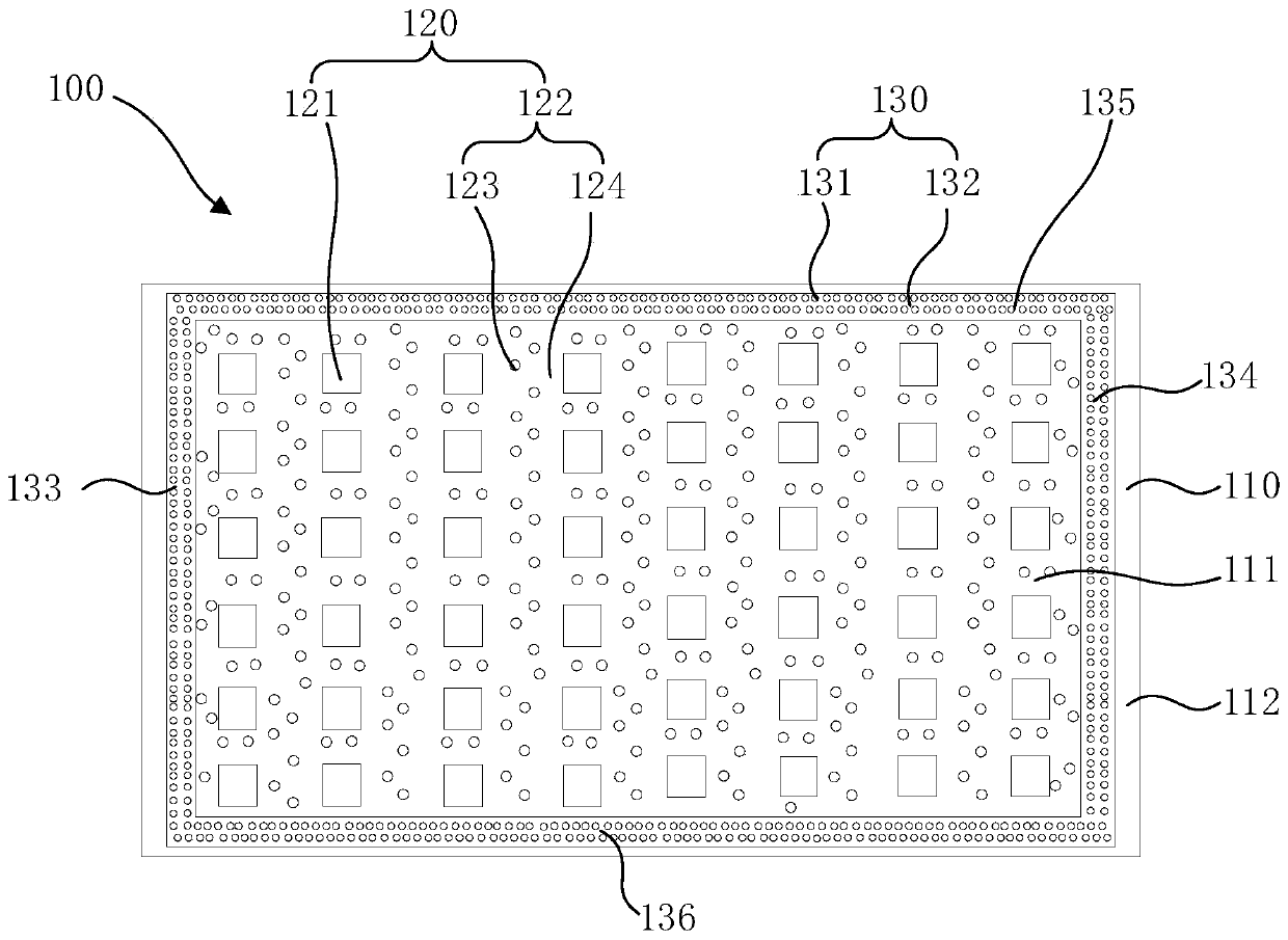
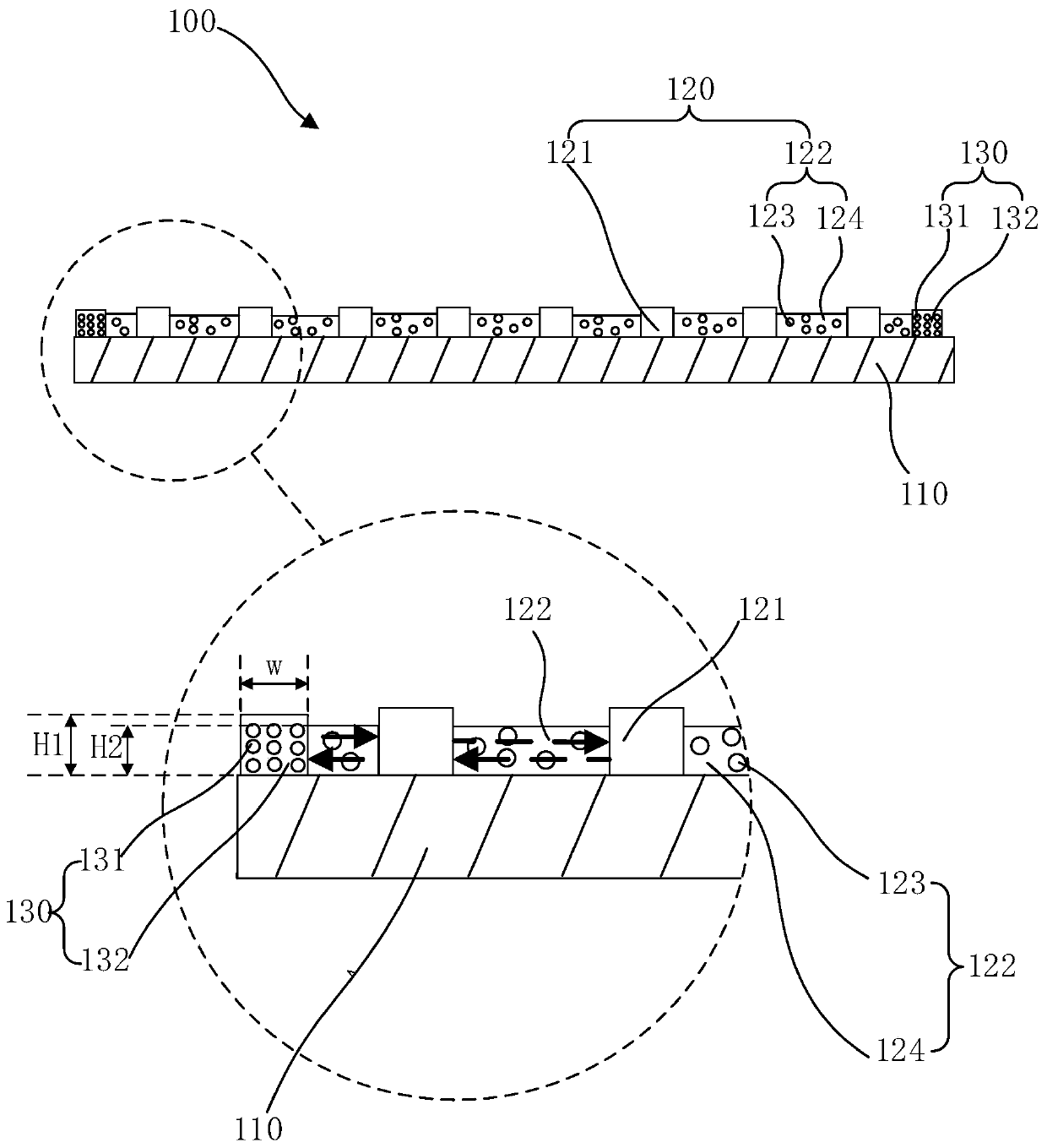
The invention relates to an LED area light source and a display device. The LED area light source comprises an LED lamp panel, a light-emitting layer and a reflection enclosing wall; the LED lamp panel comprises a light-emitting area; the light-emitting layer comprises an LED chip; the LED chip is arranged in the light-emitting area of the LED lamp panel; the reflection enclosing wall comprises reflection particles and a first transparent plastic base material; the reflection particles are distributed in the first transparent plastic base material; the reflection enclosing wall is tightly arranged on the periphery of the light-emitting layer in a surrounding mode and used for reflecting light emitted away from the light-emitting area. According to the LED surface light source and the display device of the invention, the reflection enclosing wall is tightly arranged around the periphery of the light-emitting layer in a surrounding manner; the reflection enclosing wall can reflect and recover the light emitted away from the light-emitting area; the path of the emitted light is changed; the LED light around the light-emitting area is prevented from running outwards; the brightness uniformity of the whole LED area light source is guaranteed; and the problem that the brightness of the periphery of the LED lamp panel is lower than the brightness of the center of the LED lamp panel issolved.

Description

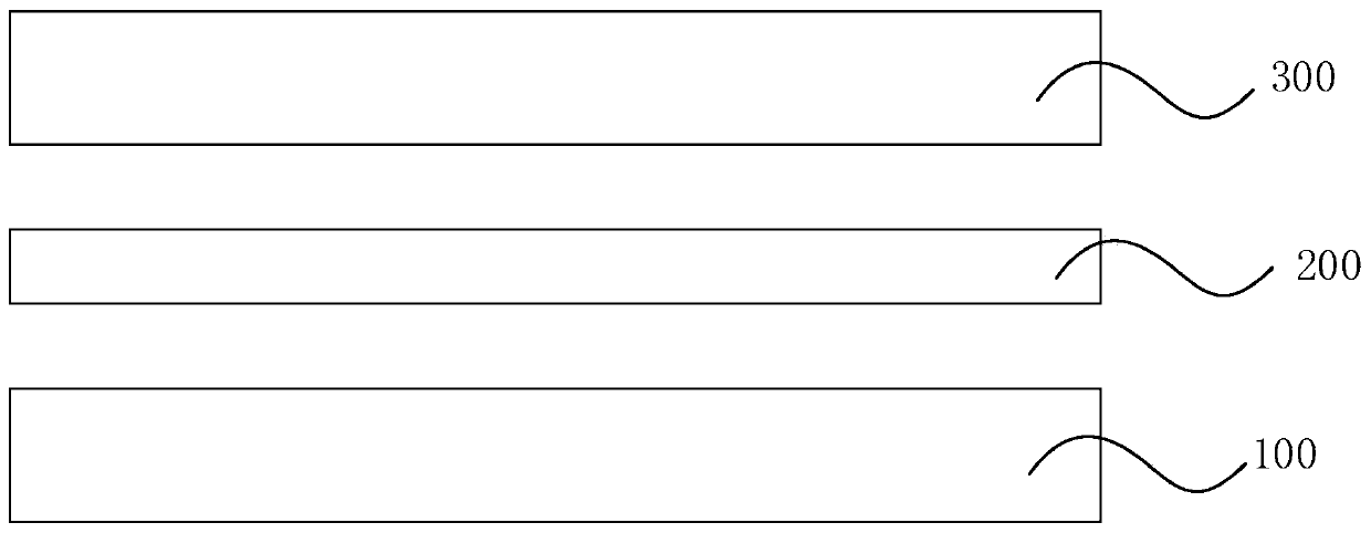
technical field [0001] The invention relates to the technical field of LED packaging and display, in particular to an LED surface light source and a display device. Background technique [0002] For traditional structural backlight sources, for example, a CSP (Chip Scale Package) module architecture or a blue light architecture that converts blue light chips into white light, such as figure 1 As shown, the LED chip is arranged on the LED lamp board, and an optical film and a liquid crystal panel are sequentially arranged above the LED chip, and the LED chip emits light to form a structural backlight. In actual testing or use, it is found that the brightness around the LED light panel is 30%-40% lower than the brightness at the center on average, which causes the overall brightness of the backlight to drop by 20%, which in turn affects the display effect. Contents of the invention [0003] Based on this, it is necessary to provide an LED surface light source and a display ...

Claims


Application Information

Patent Timeline
Patent Type & Authority Applications(China)
IPC IPC(8): H01L33/60H01L25/075G02F1/13357
CPCG02F1/133603H01L25/0753H01L33/60
Inventor 林荣松黄达人孙宜嶙
Owner INTERFACE TECH CHENGDU CO LTD
Why Eureka
Try Eureka