Preparation method of metal thin film and structure of metal thin film

A metal film and adhesion layer technology, applied in metal material coating process, coating, gaseous chemical plating and other directions, can solve the problems of excessive surface flatness difference, instability of metal film, high reflectivity, etc. Improved uniformity and consistency

Active Publication Date: 2021-12-03
YANGTZE MEMORY TECH CO LTD
View PDF8 Cites 0 Cited by
  • Summary
  • Abstract
  • Description
  • Claims
  • Application Information

AI Technical Summary

Problems solved by technology

[0004] However, for the traditional method of preparing metal thin films, the reflectance of the prepared metal thin films often has great instability, such as figure 1 As shown, when a metal thin film sample with a thickness of 480nm was formed, one abnormal sample appeared in ten samples, which had high reflectivity and high surface flatness compared with the normal sample
In addition, in some other metal thin film samples not shown, there may also be some abnormal samples whose reflectance is lower than that of normal samples
For some abnormal samples in the above two cases, their surface flatness is better / worse than normal samples, and the difference between the surface flatness of normal samples is too large, and for the semiconductor batch manufacturing process, it requires each product. The quality is similar, therefore, there is instability in the traditional method of preparing metal thin films

Method used


Image

  • Preparation method of metal thin film and structure of metal thin film
  • Preparation method of metal thin film and structure of metal thin film
  • Preparation method of metal thin film and structure of metal thin film

Examples


Embodiment Construction

[0027] Various embodiments of the invention will be described in more detail below with reference to the accompanying drawings. In the various drawings, the same elements are denoted by the same or similar reference numerals. For the sake of clarity, various parts in the drawings have not been drawn to scale.

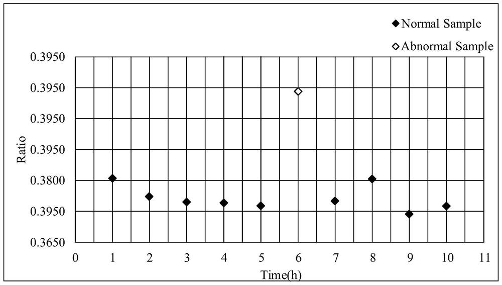
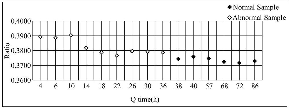
[0028] figure 2 A graph of latency versus reflectivity is shown. exist figure 2 Among them, the abscissa represents the waiting time of the sample from the formation of the adhesion layer to the completion of the growth of the metal film, in hours, and the ordinate represents the reflectivity (ratio), wherein, when the reflectivity of the sample is low, it indicates that its surface flatness is low, when The high reflectivity of the sample indicates its high surface flatness.

[0029] Depend on figure 2 From the variation trend of the middle curve, it can be known that the reflectivity of the sample is related to its waiting time, specifically, the reflectivity ...


PUM

PropertyMeasurementUnit
thicknessaaaaaaaaaa
sizeaaaaaaaaaa
sizeaaaaaaaaaa

Abstract

The application discloses a method for preparing a metal thin film and a structure of the metal thin film. The preparation method of the metal thin film comprises: forming an adhesion layer on a wafer, the wafer is located in a chamber; and passing a first precursor and a second precursor into the chamber to form a metal thin film on the surface of the adhesion layer, Wherein, before passing through the first precursor and the second precursor, the surface of the adhesion layer is pretreated to improve the component uniformity of the surface, thereby adjusting the reflectivity of the metal thin film. The preparation method of the metal thin film makes the reflectance of the metal thin film controllable by pretreating the surface of the adhesive layer, which is beneficial to improving the uniformity and consistency of the reflectance of the metal thin film, thereby facilitating the industrialized mass production of the metal thin film.

Description

technical field [0001] The invention relates to the technical field of semiconductor manufacturing, and more specifically, to a method for preparing a metal thin film and the metal thin film. Background technique [0002] With the development of semiconductor manufacturing technology, metals are widely used in semiconductor devices. Taking metal tungsten as an example, it has excellent characteristics such as low resistance, high hardness, and high melting point, and tungsten has good properties when filling trenches with high aspect ratios. Conformal and can adequately fill narrow trenches. [0003] In the preparation method of the metal thin film, a titanium nitride film (TiN film) is usually used as the adhesion layer, and a chemical vapor deposition (Chemical Vapor Deposition, CVD) deposition process is used to form the metal thin film on the adhesion layer. During the chemical vapor deposition process, multiple parameters in the process need to be monitored in real tim...

Claims


Application Information

Patent Timeline
Patent Type & Authority Patents(China)
IPC IPC(8): C23C16/14C23C16/02C23C16/34C23C16/455
CPCC23C16/0272C23C16/14C23C16/34C23C16/45525
Inventor 蔡康李昭许闵壹彭浩刘红叶微
Owner YANGTZE MEMORY TECH CO LTD
Why Eureka
Try Eureka