Preparation method of semiconductor laser cavity mask with adjustable reflectivity

A laser and semiconductor technology, which is applied in the direction of semiconductor lasers, lasers, laser components, etc., can solve the problems of poor laser damage resistance, insufficient plasma field energy and directionality, poor film compactness, etc., to achieve enhanced energy and Directionality, good effect of anti-laser damage, and controllable refractive index

Pending Publication Date: 2021-12-03
INST OF SEMICONDUCTORS - CHINESE ACAD OF SCI
View PDF14 Cites 0 Cited by
  • Summary
  • Abstract
  • Description
  • Claims
  • Application Information

AI Technical Summary

Problems solved by technology

[0003] The disadvantage of electron beam evaporation is that during the evaporation process, due to the unevenness of the material gap in the dry pot, granular defects are easily generated on the end face of the semiconductor laser. These defects greatly reduce the laser damage resistance of the end face of the semiconductor laser and affect the reliability of the laser.
The advantage of plasma-enhanced chemical vapor deposition is that it can flexibly control the composition and refractive index of the reaction-generated film, and accurately obtain the required reflectivity film; the disadvantage is that the energy and directionality of the plasma field are not strong enough, and the reaction-generated film Poor layer compactness and poor resistance to laser damage
The method of magnetron sputtering sputters two or more materials of the latter to prepare the film layer of the semiconductor laser cavity. Since the refractive index of the sputtered material is fixed, it cannot meet the requirements of laser materials with certain wavelengths or refractive indices. Reflectivity

Method used


Image

  • Preparation method of semiconductor laser cavity mask with adjustable reflectivity
  • Preparation method of semiconductor laser cavity mask with adjustable reflectivity
  • Preparation method of semiconductor laser cavity mask with adjustable reflectivity

Examples


preparation example Construction

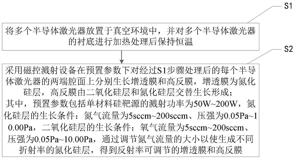
[0024] figure 1 A flow chart of a method for preparing a semiconductor laser cavity film with adjustable reflectivity according to an embodiment of the present disclosure is schematically shown. Such as figure 1 As shown, the method includes:

[0025] S1, placing a plurality of semiconductor lasers in a vacuum environment, and heating the substrates of the plurality of semiconductor lasers to maintain a constant temperature.

[0026] S2, use magnetron sputtering equipment to grow anti-reflection film and high-reflection film respectively on the cavity surfaces at both ends of each semiconductor laser processed in the step S1 under preset parameters, and the anti-reflection film is nitrided A silicon layer, the high reflection film is formed by alternately growing silicon dioxide layers and silicon nitride layers.

[0027] Wherein, the preset parameters include that the sputtering power of the single-material silicon target source is 50W-200W, the growth conditions of the si...

Embodiment 1

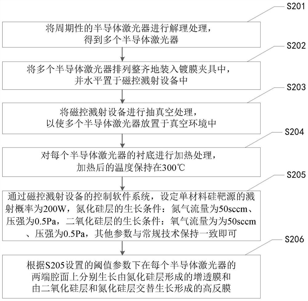
[0040] Such as figure 2 As shown, the preparation method of the semiconductor laser cavity film with adjustable reflectivity specifically includes:

[0041] S201, performing cleavage processing on periodic semiconductor lasers to obtain multiple semiconductor lasers.

[0042] S201, arrange a plurality of semiconductor lasers neatly into a coating fixture, and place them horizontally in a magnetron sputtering device.

[0043] S203, vacuumize the magnetron sputtering equipment, so that multiple semiconductor lasers are placed in a vacuum environment, and the vacuum degree of the vacuum environment is kept less than 1×10 -1 Pascal.

[0044] S204, heat treatment is performed on the substrate of each semiconductor laser, and the temperature after heating is kept at 300°C.

[0045] S205, through the software control system of the magnetron sputtering equipment, set the sputtering probability of the single-material silicon target source to 200W, the growth conditions of the silic...

Embodiment 2

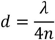
[0049] The method flow of this embodiment is consistent with that of Embodiment 1, the difference is that: the growth conditions of the silicon nitride layer are: the flow rate of nitrogen gas is 50 sccm, the pressure is 0.4 Pa, and the growth conditions of the silicon dioxide layer are: the flow rate of oxygen gas is 50 sccm, The pressure is 0.4Pa, and other threshold parameters of the device are consistent with those in Example 1. In this embodiment, taking a 1550nm semiconductor laser as an example, its equivalent refractive index is 3.2, wherein the anti-reflection coating is composed of a single layer of silicon nitride, and a silicon nitride with a refractive index of 1.79 is generated by changing the flow rate of nitrogen gas. Thin film with a thickness of 216.48nm, which can achieve a transmittance of less than 0.1%. The high-reflection film is formed by alternate growth of 5 pairs of silicon dioxide layers and silicon nitride layers. The thickness of each layer of sili...


PUM

PropertyMeasurementUnit
thicknessaaaaaaaaaa
thicknessaaaaaaaaaa
thicknessaaaaaaaaaa

Abstract

The invention provides a preparation method of a semiconductor laser cavity mask with adjustable reflectivity. The method comprises the steps: S1, a plurality of semiconductor lasers are placed in a vacuum environment, and substrates of the plurality of semiconductor lasers are heated and then kept at constant temperature; and S2, magnetron sputtering equipment is adopted to respectively grow an anti-reflection film and a high-reflection film on the cavity surfaces at the two ends of each semiconductor laser processed in the step S1 under preset parameters, the anti-reflection film is a silicon nitride layer, and the high-reflection film is formed by alternately growing a silicon dioxide layer and a silicon nitride layer, wherein the preset parameters comprise that the sputtering power of a single-material silicon target source is 50W-200W, the growth conditions of the silicon nitride layer are that the nitrogen flow is 5sccm-200sccm and the pressure intensity is 0.05 Pa-10.00 Pa, and the growth conditions of the silicon dioxide layer are that the oxygen flow is 5sccm-200sccm and the pressure intensity is 0.05 Pa-10.00 Pa, silicon nitride layers with different refractive indexes are generated by adjusting the flow of nitrogen, so that the anti-reflection film and the high-reflection film with adjustable reflectivity are obtained.

Description

technical field [0001] The disclosure relates to the field of semiconductor optoelectronic devices, in particular to a method for preparing a semiconductor laser cavity film with adjustable reflectivity. Background technique [0002] The two end faces of semiconductor lasers need to be coated with anti-reflection coating and high-reflection coating respectively. At the same time, due to the wide variety of semiconductor lasers, different types of semiconductor lasers have different lasing wavelengths and refractive indices, and the coating materials available in nature are very limited. Therefore, it brings great difficulties and challenges to the end-face coating. The conventional method is to select two or more coating materials according to the lasing wavelength and refractive index of the semiconductor laser, and perform coating through multi-layer film system design. The commonly used coating methods are: electron beam evaporation, plasma enhanced chemical vapor deposi...

Claims


Application Information

Patent Timeline
Patent Type & Authority Applications(China)
IPC IPC(8): C23C14/35C23C14/06C23C14/10C23C14/54H01S5/028
CPCC23C14/0036C23C14/0652C23C14/10C23C14/54H01S5/028
Inventor 周代兵赵玲娟梁松王圩
Owner INST OF SEMICONDUCTORS - CHINESE ACAD OF SCI
Why Eureka
Try Eureka