Flip film LED chip structure and preparation method thereof

A LED chip, flip-chip technology, used in electrical components, circuits, semiconductor devices, etc.

Inactive Publication Date: 2020-06-09
XIAMEN CHANGELIGHT CO LTD
View PDF16 Cites 1 Cited by
  • Summary
  • Abstract
  • Description
  • Claims
  • Application Information

AI Technical Summary

Problems solved by technology

[0005] In view of this, the present invention provides a flip-chip LED chip structure and its preparation method to so

Method used


Image

  • Flip film LED chip structure and preparation method thereof
  • Flip film LED chip structure and preparation method thereof
  • Flip film LED chip structure and preparation method thereof

Examples


preparation example Construction

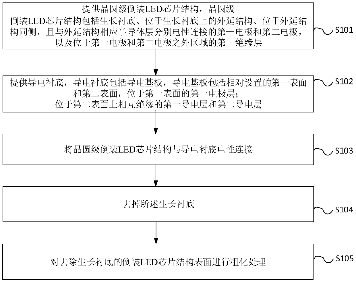
[0062] Based on this, the present invention provides a method for preparing a flip-chip thin-film LED chip structure, comprising:

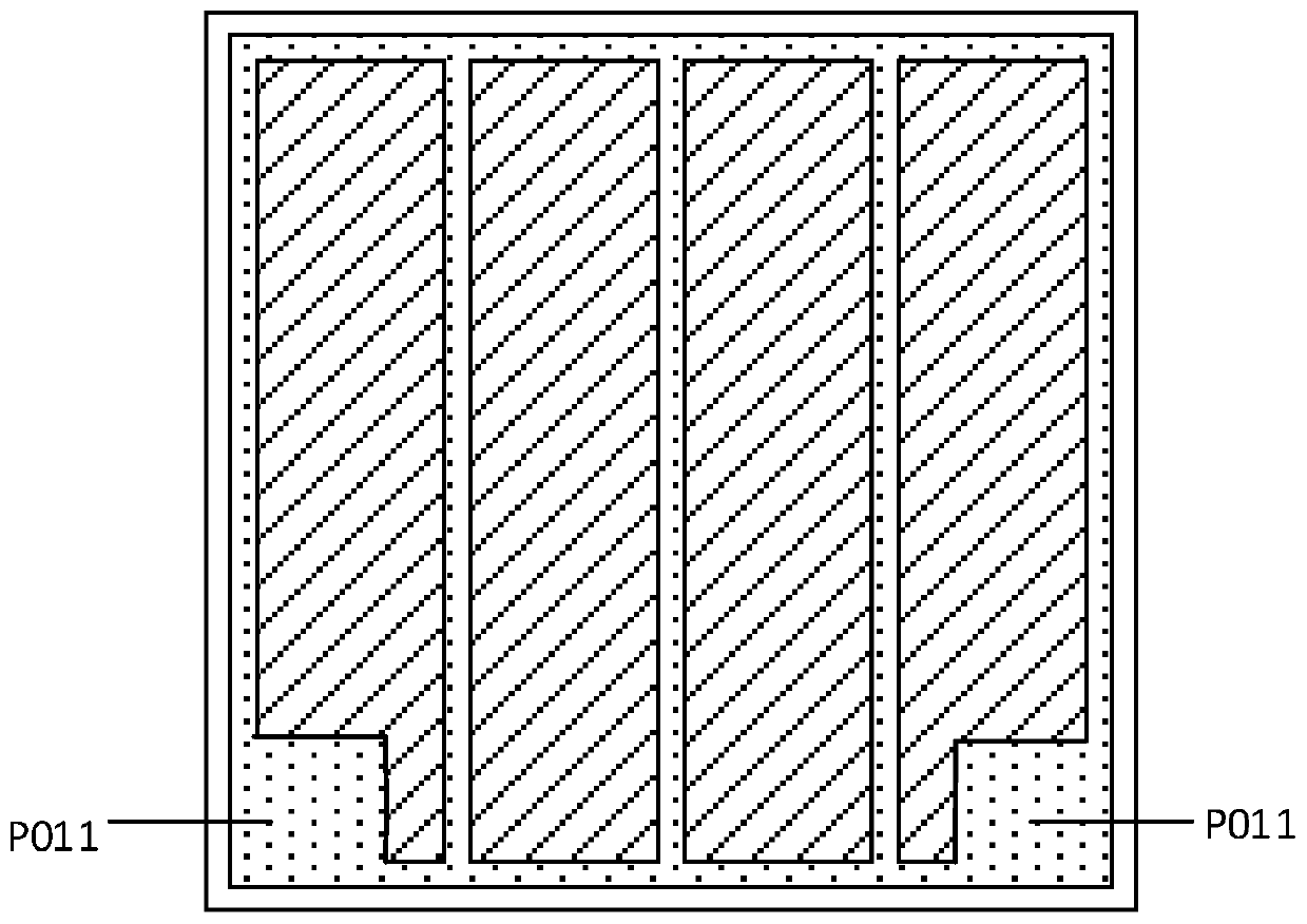
[0063] A wafer-level flip-chip LED chip structure is provided. The wafer-level flip-chip LED chip structure includes a growth substrate, an epitaxial structure located on the growth substrate, located on the same side as the epitaxial structure, and connected to the epitaxial structure. a first electrode and a second electrode electrically connected respectively, and a first insulating layer located outside the first electrode and the second electrode;

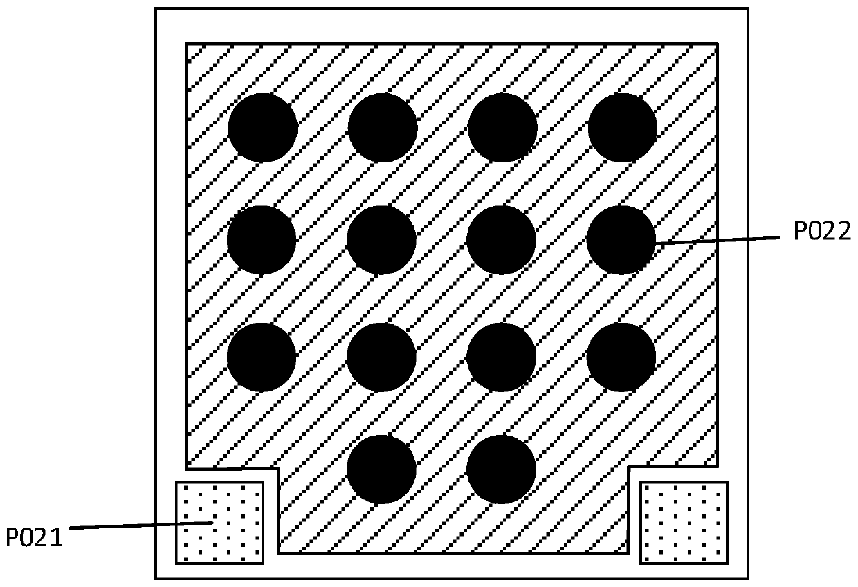
[0064] Provide a conductive substrate, the conductive substrate includes a conductive substrate, the conductive substrate includes a first surface and a second surface oppositely arranged; a first electrode layer located on the first surface of the conductive substrate; a first electrode layer located on the second surface of the conductive substrate The first conductive layer and the second condu...


PUM


Abstract

The invention provides a flip film LED chip structure and a preparation method thereof. According to the preparation method, a flip LED chip structure with a first electrode and a second electrode, and a conductive substrate with a first conductive layer and a second conductive layer are provided; the area of the conductive substrate is larger than that of the flip LED chip; the first electrode iselectrically connected with a first conductive layer; the second electrode is electrically connected with a second conductive layer; the area of the second conductive layer is larger than that of thesecond electrode; the area outside the area, connected with the second electrode, of the second conductive layer serves as a second electrode layer and is used for being electrically connected with an external circuit. According to the flip film LED chip structure formed by the preparation method, the maximum light-emitting area of the LED chip is ensured; and roughening treatment can be carriedout on a surface without a growth substrate, so that the light-emitting distribution of the LED chip is improved, and the light-emitting efficiency of the LED chip is improved.

Description

technical field [0001] The invention relates to the technical field of manufacturing semiconductor devices, in particular to a flip-chip thin-film LED chip structure and a preparation method thereof. Background technique [0002] A light emitting diode (Light Emitting Diode, referred to as LED) is a semiconductor solid-state light-emitting device, which is made by using the principle of semiconductor P-N junction electroluminescence. LED devices have good photoelectric properties such as low turn-on voltage, small size, fast response, good stability, long life, and no pollution. [0003] LED chips are divided into positive LED chips, flip LED chips and vertical LED chips according to their structure. Among them, the vertical LED chip is a high-performance LED chip, which has the advantages of high light efficiency, good heat dissipation, and high reliability. It is generally used to prepare high-power, high-brightness and excellent performance LED chips; Light-transmitting...

Claims


Application Information

Patent Timeline
IPC IPC(8): H01L33/62H01L33/48H01L33/38
CPCH01L33/38H01L33/48H01L33/62
Inventor 赵斌曲晓东杨克伟林志伟陈凯轩
Owner XIAMEN CHANGELIGHT CO LTD
Why Eureka
Try Eureka