Cutting method for reducing cutting loss of LED chip

A technology of LED chip and cutting method, which is applied in the direction of electrical components, circuits, semiconductor devices, etc., and can solve the problems of large loss of light-emitting area of ​​the chip, increase of contact area between the back of the blade and the surface of the chip, and cracking, etc.

Active Publication Date: 2020-12-29
SHANDONG INSPUR HUAGUANG OPTOELECTRONICS
View PDF10 Cites 1 Cited by
  • Summary
  • Abstract
  • Description
  • Claims
  • Application Information

AI Technical Summary

Problems solved by technology

This method of operation is a typical mechanical cutting. The disadvantage is that the full-thickness cutting along the half-cut cutting path, the height of the knife must be reduced

Method used


Image

  • Cutting method for reducing cutting loss of LED chip

Examples


Embodiment 1

[0064] Step 1: Prepare the LED chip;

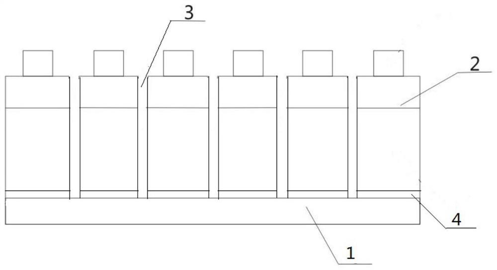
[0065] Step 2: Take the prepared LED chip, and cut the P side of the LED chip into half at intervals according to the period set by the process; the cutting depth is 5% of the thickness of the LED chip;

[0066] Step 3: Take the half-cut LED chip and test it with a testing machine. The test current is 20mA, the test time is 5ms, and the corresponding brightness, voltage and wavelength of the LED chip are tested;

[0067] Step 4: Adsorb the tested LED chip on the suction cup of the glue homogenizer, use the glue homogenizer to apply negative glue on the P surface, and form a protective film on the P surface after coating; the speed of the glue homogenizer suction cup is first 2500r / 3000r / min after min, the glue thickness is

[0068] Step 5: Place the glue-coated LED chip on the platform of the photolithography machine for light exposure, and expose the cutting line on the protective film; the light intensity during exposure is 6 μW / cm ...

Embodiment 2

[0079] Step 1: Prepare the LED chip;

[0080] Step 2: Take the prepared LED chip, and cut the P side of the LED chip into half at intervals according to the period set by the process; the cutting depth is 8% of the thickness of the LED chip;

[0081] Step 3: Take the half-cut LED chip and test it with a testing machine. The test current is 20mA, the test time is 5ms, and the corresponding brightness, voltage and wavelength of the LED chip are tested;

[0082]Step 4: Adsorb the tested LED chip on the suction cup of the glue homogenizer, and use the glue homogenizer to apply negative glue on the P surface, and form a protective film on the P surface after the glue is applied; the speed of the glue homogenizer suction cup is first 3000r / 4000r / min after min, the glue thickness is

[0083] Step 5: Place the glue-coated LED chip on the platform of the photolithography machine for light exposure, and expose the cutting line on the protective film; the light intensity during expos...

Embodiment 3

[0094] Step 1: Prepare the LED chip;

[0095] Step 2: Take the prepared LED chip, and cut the P side of the LED chip into half at intervals according to the period set by the process; the cutting depth is 10% of the thickness of the LED chip;

[0096] Step 3: Take the half-cut LED chip and test it with a testing machine. The test current is 20mA, the test time is 5ms, and the corresponding brightness, voltage and wavelength of the LED chip are tested;

[0097] Step 4: Adsorb the tested LED chip on the suction cup of the glue homogenizer, use the glue homogenizer to apply negative glue on the P surface, and form a protective film on the P surface after coating; the speed of the glue homogenizer suction cup is first 4000r / 5000r / min after min, the glue thickness is

[0098] Step 5: Place the glue-coated LED chip on the platform of the photolithography machine for light exposure, and expose the cutting line on the protective film; the light intensity during exposure is 10μW / cm...


PUM


Abstract

The invention discloses a cutting method for reducing the cutting loss of an LED chip. The method comprises steps of firstly carrying out the half-cutting of a P surface of the chip, carrying out thetesting through a testing machine, and facilitating the output of photoelectric parameters, such as brightness, voltage and wavelength, of the chip; coating photoresist on the P surface of the chip byusing a spin coater to form a shielding film, exposing and developing the P surface of the chip, and corroding and exposing a cutting channel; coating photoresist on the N surface of the chip to protect the metal on the N surface and facilitate subsequent dry etching; washing off the shielding film on the P surface, pasting a blue film, finally washing off the adhesive film on the N surface, pouring the film, and finishing the cutting operation. According to the cutting method for reducing the cutting loss of the LED chip, the N-surface adhesive film design is utilized, and dry etching is matched, so situations of edge breakage, wafer flying and the like during chip cutting are effectively avoided, cutting loss of the chip is reduced, meanwhile, light emitting efficiency of tube core particles is guaranteed, the product yield is increased, and practicability is high.

Description

technical field [0001] The invention relates to the technical field of LED manufacturing, in particular to a cutting method for reducing cutting loss of LED chips. Background technique [0002] Due to its high luminous efficiency, wide color range, and long service life, LED chips have been widely valued in the semiconductor lighting industry, and have been widely used in various fields such as display screens, traffic lights, landscape lighting, and automotive status displays. Especially in recent years, with the development of technology and breakthroughs, the small-pitch screens used for mobile phones, outdoor displays, etc. However, the requirements for products are getting smaller and smaller, and the LED core is facing higher requirements. While the size of the core is reduced to further increase the output, the luminous brightness of the core must also maintain a high test result. The manufacturing process of the die puts forward more stringent requirements. [0003...

Claims


Application Information

Patent Timeline
IPC IPC(8): H01L33/00H01L21/302H01L21/266
CPCH01L21/266H01L21/302H01L33/005
Inventor 郑军李琳琳齐国健
Owner SHANDONG INSPUR HUAGUANG OPTOELECTRONICS
Why Eureka
Try Eureka