Display substrate and display device

A technology for display substrates and display devices, which is applied in semiconductor devices, electrical components, circuits, etc., and can solve problems such as affecting display effects, missed detection of bright spots, and ET twill

Active Publication Date: 2020-06-19
BOE TECH GRP CO LTD +1
View PDF6 Cites 1 Cited by
  • Summary
  • Abstract
  • Description
  • Claims
  • Application Information

AI Technical Summary

Problems solved by technology

[0004] Embodiments of the present disclosure provide a display substrate and a display device, which can effectively improve the brightness difference between sub-pixels of the same col

Method used


Image

  • Display substrate and display device
  • Display substrate and display device
  • Display substrate and display device

Examples


Embodiment 1

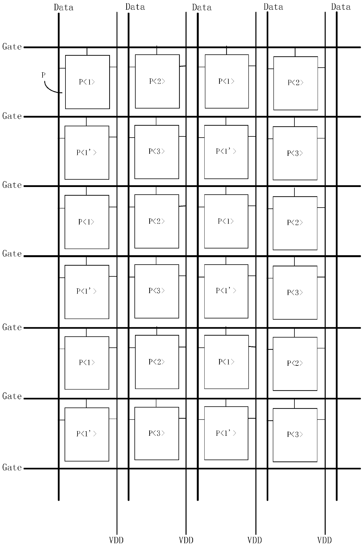
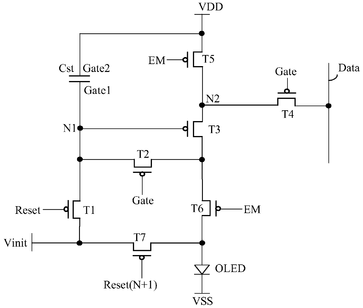
[0084] Image 6 It is a schematic structural diagram of a first sub-pixel in each pixel unit in Embodiment 1 of the present disclosure, Figure 7 It is a schematic structural diagram of another first sub-pixel in each pixel unit in Embodiment 1 of the present disclosure. In order to effectively solve the technical problems in the comparative embodiment, Embodiment 1 of the present disclosure provides a comparison with the foregoing comparative embodiment. Different settings of the film layer structure of the first sub-pixel, specifically, the difference between Embodiment 1 of the present disclosure and the foregoing comparative embodiment is that in Embodiment 1 of the present disclosure, as figure 1 , figure 2 , Image 6 with Figure 7 As shown, for each first sub-pixel (such as P or P), the first sub-pixel (such as P or P) also includes a setting corresponding to the through hole h In the first sub-pixel (such as P or P), the orthographic projection of the second plate...

Embodiment 2

[0095] Figure 8 It is a schematic structural diagram of a first sub-pixel in each pixel unit in Embodiment 2 of the present disclosure, Figure 9It is another schematic structural diagram of a first sub-pixel in each pixel unit in Embodiment 2 of the present disclosure. In order to effectively solve the technical problems in the comparative embodiment, Embodiment 2 of the present disclosure provides Different setting of the film layer structure of the first sub-pixel, specifically, the difference between the second embodiment of the present disclosure and the aforementioned comparative embodiment is that in the second embodiment of the present disclosure, for each pixel unit, such as figure 1 , figure 2 with Figure 8 As shown, in a first sub-pixel P of the pixel unit, the anode AND of the light-emitting device OLED is located on the side of the second plate Gate2 away from the substrate, and the anode AND is on the first plate Gate1 The orthographic projection of covers ...

Embodiment 3

[0108] Figure 10 It is a schematic structural diagram of a first sub-pixel in each pixel unit in Embodiment 3 of the present disclosure, Figure 11 It is a schematic structural diagram of another first sub-pixel in each pixel unit in Embodiment 3 of the present disclosure. In order to effectively solve the technical problems in the comparative embodiment, Embodiment 3 of the present disclosure provides a comparison with the foregoing comparative embodiment. Different setting of the film layer structure of the first sub-pixel, specifically, the difference between the third embodiment of the present disclosure and the aforementioned comparative example is: in the third embodiment of the present disclosure, as figure 1 , figure 2 , Figure 10 with Figure 11 As shown, for each first sub-pixel (such as P or P), in the first sub-pixel (such as P or P), the light emitting device OLED The anode AND is located on the side of the second plate Gate2 away from the substrate, and th...


PUM


Abstract

The invention provides a display substrate. The display substrate comprises a substrate base plate and a plurality of pixel units located on the substrate base plate. Each pixel unit comprises two first sub-pixels, a second sub-pixel and a third sub-pixel, each sub-pixel comprises a storage capacitor which comprises a first polar plate and a second polar plate which are oppositely arranged, through holes are formed in the second polar plates, and the first sub-pixels further comprise shielding metal structures arranged corresponding to the through holes; in the first sub-pixels, the shieldingmetal structures are connected with the second polar plates; the orthographic projections of the second polar plates and the shielding metal structures on the substrate base plate cover the orthographic projections of the first polar plates on the substrate base plate, and the orthographic projections of the shielding metal structures on the substrate base plate cover the orthographic projectionsof the through holes on the substrate base plate. The invention further provides a display device.

Description

technical field [0001] Embodiments of the present disclosure relate to the field of display technologies, and in particular, to a display substrate and a display device. Background technique [0002] The GGRB pixel structure is one of the mainstream pixel structures currently used in Organic Light-Emitting Diode (OLED) display devices, that is, each pixel of an OLED display device includes a green sub-pixel G, a green sub-pixel G, a red sub-pixel Subpixel R and blue subpixel B. [0003] In each pixel of the OLED display device, the film layer structures in the two green sub-pixels G are inconsistent, resulting in a brightness difference between the two green sub-pixels G, specifically, in the two green sub-pixels G, The inconsistency of the parasitic capacitance between the storage capacitor and the anode leads to a brightness difference between the two green sub-pixels G. For the entire OLED display device, the brightness difference between the green sub-pixels G is likely...

Claims


Application Information

Patent Timeline
IPC IPC(8): H01L27/32H01L51/52
CPCH10K59/35H10K59/126H10K59/131H10K50/813
Inventor 邓雷魏悦张震邓伟邹富伟黎飞潘康观
Owner BOE TECH GRP CO LTD
Why Eureka
Try Eureka