Integrated structure of crystal resonator and control circuit and integration method thereof

A crystal resonator and control circuit technology, which is applied to circuits, semiconductor devices, electric solid-state devices, etc., can solve problems such as difficult integration and large size

Active Publication Date: 2020-07-07
NINGBO SEMICON INT CORP
View PDF11 Cites 2 Cited by
  • Summary
  • Abstract
  • Description
  • Claims
  • Application Information

AI Technical Summary

Problems solved by technology

[0005] The purpose of the present invention is to provide an integration method of a crystal resonator and a control circuit, so as to solve the problem that the existing crystal resonator has a large size and is not easy to integrate

Method used


Image

  • Integrated structure of crystal resonator and control circuit and integration method thereof
  • Integrated structure of crystal resonator and control circuit and integration method thereof
  • Integrated structure of crystal resonator and control circuit and integration method thereof

Examples


Embodiment 2

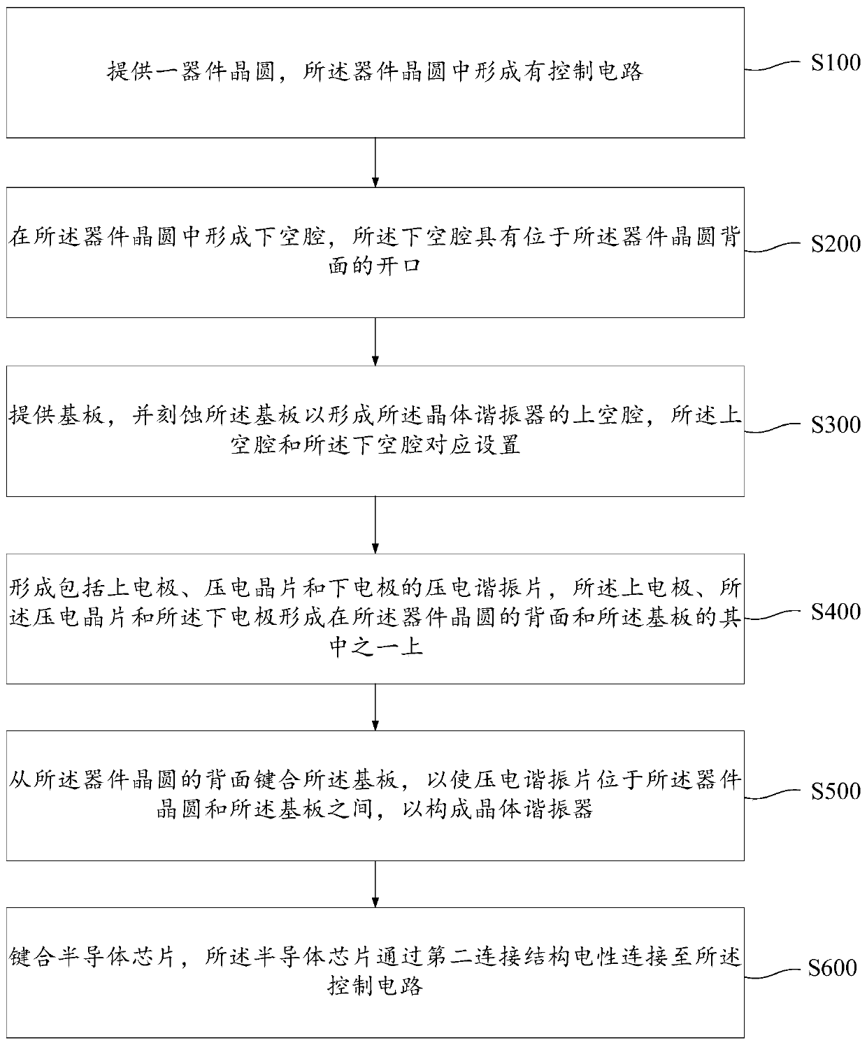
[0161] The difference from Embodiment 1 is that in this embodiment, the upper electrode 530, the piezoelectric wafer 520 and the lower electrode 510 of the piezoelectric resonant plate 500 are all formed on the back surface of the device wafer 100, and the The piezoelectric resonator plate 500 covers the opening of the lower cavity 120, and the formed crystal resonator is electrically connected to the control circuit in the device wafer 100, and then the bonding process is performed so that the upper cavity 310 corresponds to the The side of the piezoelectric resonator plate 500 facing away from the lower cavity 120 constitutes a crystal resonator, thereby realizing the integrated arrangement of the crystal resonator and the control circuit.

[0162] In this embodiment, the method of providing a device wafer with a control circuit and forming a lower cavity in the device wafer can refer to Embodiment 1, which will not be repeated here.

[0163] And, the method for forming the ...

Embodiment 1

[0179] In Embodiment 1 and Embodiment 2, the piezoelectric resonant plates including the upper electrode, the piezoelectric wafer and the lower electrode are all formed on the substrate or the device wafer. The difference from the above embodiment is that in this embodiment, the upper electrode and the piezoelectric wafer are formed on the substrate, and the lower electrode is formed on the device wafer.

[0180] Figure 3a ~ Figure 3d It is a schematic structural diagram of the method for integrating the crystal resonator and the control circuit in the third embodiment of the present invention during its preparation process. The steps of forming the crystal resonator in this embodiment will be described in detail below with reference to the accompanying drawings.

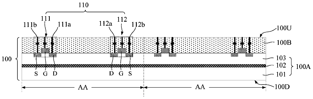
[0181] first reference Figure 3a As shown, a device wafer 100 is provided, and a control circuit is formed in the device wafer 100, and a lower electrode 510 is formed on the back surface of the device wafer 100,...

Embodiment 4

[0198] The difference from the above embodiment is that in this embodiment, before the device wafer and the substrate are bonded to each other, the semiconductor chip is bonded to the back surface of the device wafer, and the semiconductor chip and the control circuit are connected through the second connection structure. electrical connection. And, in this embodiment, the explanation will be made by taking the lower electrode, the piezoelectric wafer and the upper electrode of the piezoelectric resonant plate all formed on the device wafer as an example.

[0199] First, refer to Figure 4a As shown, a device wafer 100 is provided having control circuits formed therein. And, the first conductive plug, the first connection line, the second conductive plug and the second connection line of the first connection structure are also formed in the device wafer, as well as the conductive plugs and the second connection structure in the second connection structure. connection line. ...


PUM


Abstract

The invention provides an integrated structure of a crystal resonator and a control circuit, and an integration method thereof. A lower cavity is formed in a device wafer on which a control circuit isformed, an upper cavity is formed in a substrate, and the device wafer and the substrate are bonded by using a bonding process, so that a piezoelectric resonance piece is clamped between the device wafer and the substrate, and the integrated arrangement of the crystal resonator and the control circuit is realized. Moreover, the semiconductor chip can be further bonded to the back surface of the same device wafer, so the integration level of the crystal resonator is further improved, and parameters of the on-chip modulation crystal resonator are realized. Compared with a traditional crystal resonator, the crystal resonator has the advantages that the size is smaller, the power consumption of the crystal resonator can be reduced, the crystal resonator can be integrated with other semiconductor components more easily, and therefore the integration degree of the device can be improved.

Description

technical field [0001] The invention relates to the technical field of semiconductors, in particular to an integrated structure of a crystal resonator and a control circuit and an integrated method thereof. Background technique [0002] Crystal resonators are resonant devices made using the inverse piezoelectric effect of piezoelectric crystals. They are key components of crystal oscillators and filters. They are widely used in high-frequency electronic signals to achieve accurate timing, frequency standards, and filtering. An essential frequency control function in signal processing systems. [0003] With the continuous development of semiconductor technology and the popularization of integrated circuits, the size of various components tends to be miniaturized. However, the current crystal resonator is not only difficult to integrate with other semiconductor components, but also the size of the crystal resonator is large. [0004] For example, currently common crystal res...

Claims


Application Information

Patent Timeline
Patent Type & Authority Applications(China)
IPC IPC(8): H03H9/205H03H3/02
CPCH03H9/205H03H3/02H03H9/173H03H9/105H03H9/0557H03H2003/021H03H9/0542H10N39/00H10N30/071H03H9/19
Inventor 秦晓珊
Owner NINGBO SEMICON INT CORP
Why Eureka
Try Eureka