Free space two-dimensional array detector
A two-dimensional array and free space technology, applied in the direction of electric solid-state devices, semiconductor devices, semiconductor/solid-state device components, etc., can solve the problems of excessively long wires and easy short circuits, so as to improve reliability and avoid excessively long wires Effect
- Summary
- Abstract
- Description
- Claims
- Application Information
AI Technical Summary
Problems solved by technology
Method used
Image

Examples
Embodiment 1
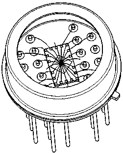
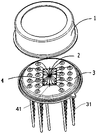
[0043] like Figure 1-5 As shown, this embodiment takes a 4×4 free-space two-dimensional array detector as an example for illustration:
[0044] The detector chip 2 in this embodiment is a 4×4 two-dimensional array detector chip, and the detector chip 2 is rectangular.
[0045] The detector chip 2 includes 20 bonding pads, including 16 positive electrode bonding pads and 4 negative electrode bonding pads.
[0046] The heat sink 4 is rectangular.
[0047] There are 18 conductive contacts 41 on the heat sink 4 . The conductive contacts 41 are distributed on the four sides of the rectangle, and the conductive contacts 41 are symmetrical to the central axis of the rectangle (including the central axis connecting the central points of the long sides and the central axis connecting the central points of the short sides). Specifically, four conductive contacts 41 are provided on the long side, three conductive contacts 41 are provided on the short side, and one conductive contact ...
Embodiment 2
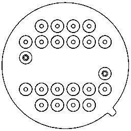
[0053] like Figure 6-10 As shown, this embodiment takes a 3×3 free-space two-dimensional array detector as an example for illustration:
[0054] The detector chip 2 in this embodiment is a 3×3 two-dimensional array detector chip, and the detector chip 2 is square. The detector chip 2 includes 9 positive pads and 3 negative pads.
[0055] The heat sink 4 is a square.
[0056] There are 12 conductive contacts 41 corresponding to the 12 pads on the detector chip 2 . The conductive contacts 41 are distributed on the edges of the square, and three conductive contacts are arranged on each side of the square.
[0057]The pins of the detector chip 2 are evenly distributed on the four sides of the first square, the conductive contacts 41 are evenly distributed on the four sides of the second square, and the pins 31 are evenly distributed on the four sides of the third square. , the centers of the second square and the third square are the same and the four sides of the first squar...
Embodiment 3
[0059] like Figure 11 As shown, this embodiment takes another pin arrangement form of a 3×3 free-space two-dimensional array detector as an example for illustration:
[0060] The pins of the detector chip 2 are evenly distributed on the first circle, the conductive contacts 41 are evenly distributed on the second circle, and the pins 31 are evenly distributed on the third circle. The first circle, the second circle and the third circle are concentric circles.
[0061] The heat sink 4 is circular, and the heat sink 4 is concentric with the first circle.
PUM
 Abstract
Description
Claims
Application Information
 - R&D
- Intellectual Property
- Life Sciences
- Materials
- Tech Scout
- Unparalleled Data Quality
- Higher Quality Content
- 60% Fewer Hallucinations
Browse by: Latest US Patents, China's latest patents, Technical Efficacy Thesaurus, Application Domain, Technology Topic, Popular Technical Reports.
© 2025 PatSnap. All rights reserved.Legal|Privacy policy|Modern Slavery Act Transparency Statement|Sitemap|About US| Contact US: help@patsnap.com