Vertical-cavity surface-emitting semiconductor laser structure

A vertical cavity surface emission and laser technology, applied in the direction of semiconductor lasers, lasers, laser components, etc., can solve the problems of reducing VCSEL performance, thermal lens effect of space burning holes, affecting the uniformity of current injection, etc., to reduce space burning holes Phenomena and the probability of occurrence of thermal lensing, the effect of reducing parasitic capacitance and improving performance

Active Publication Date: 2020-07-21
INST OF SEMICONDUCTORS - CHINESE ACAD OF SCI
View PDF11 Cites 2 Cited by
  • Summary
  • Abstract
  • Description
  • Claims
  • Application Information

AI Technical Summary

Benefits of technology

The inventors have developed an improved type of Vertically Cavity Surface Emission Lasers (VCES) with better efficiency compared to previous designs by creating tiny oxygenated areas on top or around certain parts of its structure. This results in more consistently injected currents without causing damage during operation due to heat buildup caused by hot spots. Additionally, this design allows for increased power output while maintaining good optics properties over longer periods of time.

Problems solved by technology

Technological Problem: The technical issue addressed in this patents relates to improving the performance and cost reduction required for efficient transmission of signals over shorter distances at speeds greater than 1 GHz. Current methods like wavelength division multiplexing require expensive equipment and involve complicated processes. Existing techniques include vapor phase epilayer deposition, ion implantation, and coating metal plasma mirror surfaces onto carrier layers. However these conventional ways face challenges due to their limitations including slow response time, poor scalability, difficulty integrating them within chip designs, limited application range, and lacked versatile options for connecting electronic components together.

Method used


Image

  • Vertical-cavity surface-emitting semiconductor laser structure
  • Vertical-cavity surface-emitting semiconductor laser structure

Examples


Embodiment Construction

[0035] In order to make the object, technical solution and advantages of the present invention clearer, the present invention will be further described in detail below in conjunction with specific embodiments and with reference to the accompanying drawings.

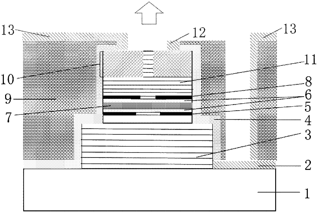
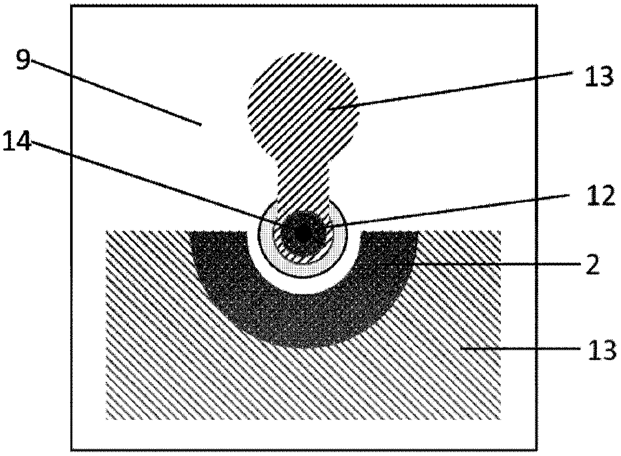
[0036] According to the vertical cavity surface emitting semiconductor laser structure provided by the present invention, an embodiment of the present invention provides a 850nm high-speed vertical cavity surface emitting laser, figure 1 A cross-sectional structure diagram of an 850nm high-speed vertical cavity surface emitting laser in an embodiment of the present invention is shown, figure 2 Its top view structure diagram. refer to figure 1 and figure 2 , the 850nm high-speed vertical cavity surface emitting laser provided by the embodiment of the present invention includes:

[0037] The substrate 1 is made of GaAs.

[0038] The N surface electrode 2 is made of Au / Ge / Ni metal and has a semi-circular structure.

...


PUM

PropertyMeasurementUnit
Apertureaaaaaaaaaa

Abstract

The invention discloses a vertical-cavity surface-emitting semiconductor laser structure, and the structure comprises: an optical oxidation limiting layer which is located at a standing wave antinodeof a laser and plays an optical limiting role; an electrical oxidation limiting layer which is located at the standing wave node of the laser and plays a role in limiting current; a proton injection layer which is positioned on the electrical oxidation limiting layer and the optical oxidation limiting layer and is used for increasing the information transmission rate of the laser; and a buffer layer epitaxially grown on the substrate, wherein an N-surface electrode, an N-type DBR, an N-type space layer, an active region, a P-type space layer, a P-type DBR layer and a P-surface electrode form alaser resonant cavity. The vertical-cavity surface-emitting laser adopts a proton injection and separation limited oxidation structure, the structure improves the uniformity of current injection, reduces the parasitic capacitance of the device, has the low threshold current and stable single-transverse-mode or multi-transverse-mode output, and improves the high-speed performance of the device.

Description


Claims


Application Information

Patent Timeline
Owner INST OF SEMICONDUCTORS - CHINESE ACAD OF SCI
Why Eureka
Try Eureka