
A bias circuit independent irrelevant to power supply voltage

A bias circuit and power supply voltage technology, applied in the direction of adjusting electrical variables, control/regulation systems, instruments, etc., can solve the problems of output bias current deviation, current change can not be ignored, etc., to reduce the change, the minimum operating power supply voltage is low , The effect of a large working power supply voltage range

Inactive Publication Date: 2020-08-11
SHENZHEN BAITAI IND CO LTD
View PDF5 Cites 0 Cited by
  • Summary
  • Abstract
  • Description
  • Claims
  • Application Information

AI Technical Summary

Problems solved by technology

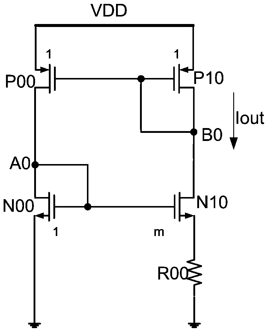
[0006] For the above-mentioned traditional bias circuit, in the case of a relatively large power supply voltage variation range, there is a large difference in the potential of nodes A0 and B0. Due to the channel length modulation effect, the currents of PMOS transistors P0 and P1 are not equal, which will cause the output The deviation of the bias current; therefore, the current change caused by the channel length modulation effect cannot be ignored, as shown in equation (2):

Method used


Image

  • A bias circuit independent irrelevant to power supply voltage
  • A bias circuit independent irrelevant to power supply voltage
  • A bias circuit independent irrelevant to power supply voltage

Examples


Embodiment Construction

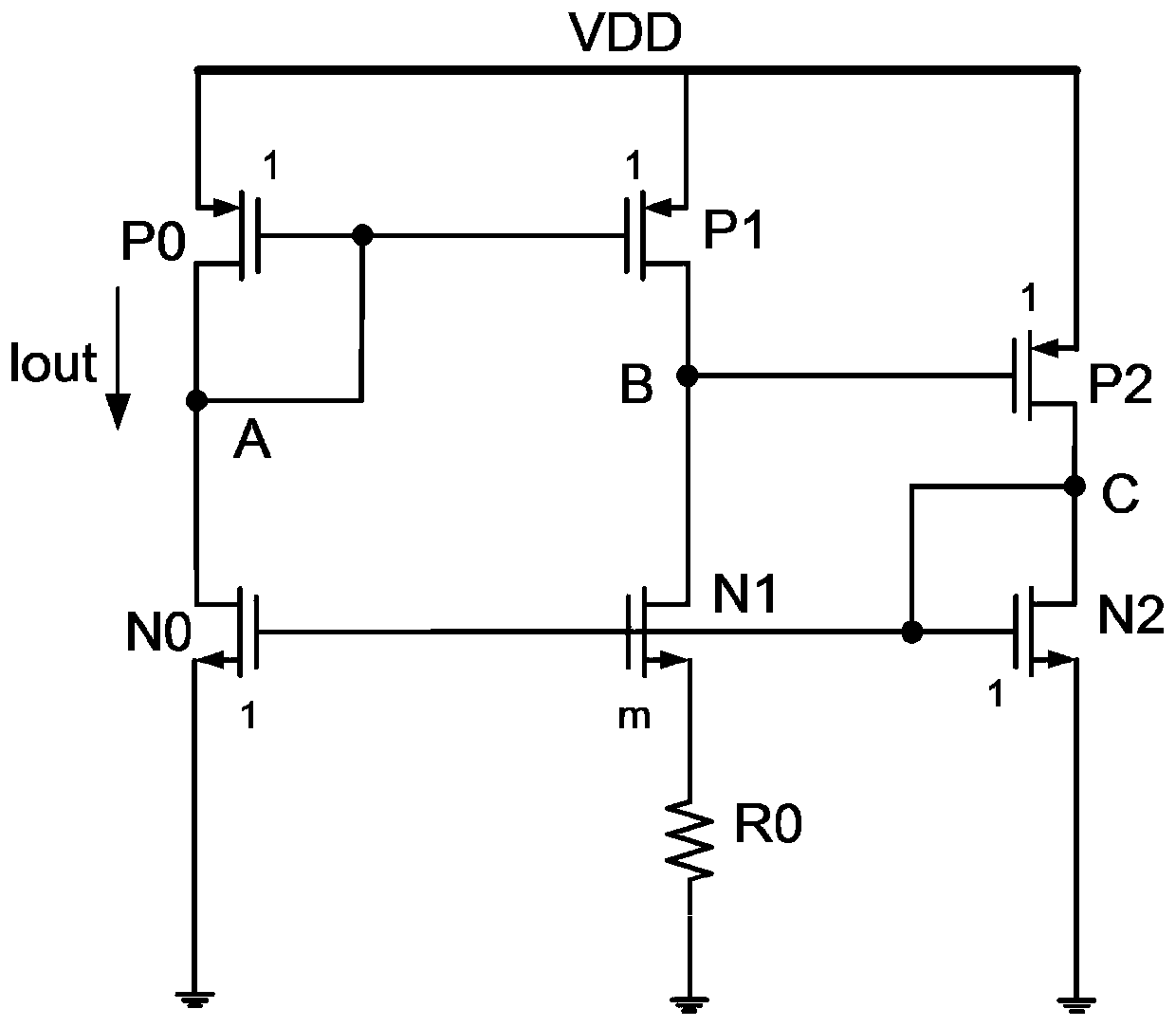
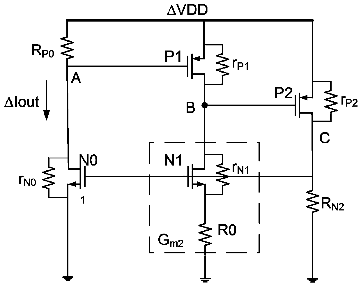
[0025] In this example, if figure 2 As shown, a bias circuit independent of power supply voltage, including:

[0026] Three PMOS transistors: the first PMOS transistor P0, the second PMOS transistor P1, and the third PMOS transistor P2; three NMOS transistors: the first NMOS transistor N0, the second NMOS transistor N1, the third NMOS transistor N2 and a resistor R0;

[0027] The source of the first NMOS transistor N0 is grounded; the drain of the first NMOS transistor N0 is connected to the gate and drain of the first PMOS transistor P0, and the gate of the second PMOS transistor P1 is connected to point A;

[0028] Both the source of the first PMOS transistor P0 and the source of the second PMOS transistor P1 are connected to the power supply VDD; the first PMOS transistor P0 is connected in a diode structure, and forms a current mirror with the second PMOS transistor P1;

[0029] The source of the third NMOS transistor N2 is grounded, the gate and drain of the third NMOS ...


PUM


Abstract

The invention discloses a bias circuit irrelevant to power supply voltage, which comprises three PMOS (P-channel Metal Oxide Semiconductor) tubes, three NMOS (N-channel Metal Oxide Semiconductor) tubes and a resistor R0, and the first PMOS tube P0 is connected into a diode structure and forms a current mirror with a second PMOS tube P1; the third NMOS tube N2 is connected into a diode structure and forms a current mirror with the first NMOS tube N0; and the source electrode of the third PMOS tube P2 is connected to the power supply VDD and forms a current branch with the third NMOS tube N2. According to the invention, the influence of the power supply voltage change on the bias current can be reduced to the greatest extent, so that the change of the system quiescent current along with thepower supply voltage can be effectively reduced.

Description

technical field [0001] The invention belongs to the technical field of integrated circuits, in particular to a bias circuit independent of power supply voltage. Background technique [0002] With the advancement of CMOS technology, the development trend of integrated circuits is higher and higher integration, lower power supply voltage and lower power consumption; low-voltage and low-power consumption design is the mainstream direction of integrated circuit development. With the rapid development of integrated circuits, its application fields are also expanding. In some application fields such as industrial control, the power supply voltage varies widely, which requires that the design of the chip not only has low power consumption, but also can adapt to the needs of wide power supply voltage. [0003] The bias circuit provides a quiescent operating point and a bias current for other devices in the circuit to perform specific functions; to a certain extent, the magnitude of ...

Claims


Application Information

Patent Timeline
Patent Type & Authority Applications(China)
IPC IPC(8): G05F3/26
CPCG05F3/262
Inventor 方成权磊贾晨尹勇生
Owner SHENZHEN BAITAI IND CO LTD
Learn More