An anti-jamming circuit board and terminal

A circuit board and circuit layer technology, applied in the direction of circuits, printed circuits, printed circuits, etc., can solve problems such as complexity, limited magnetometer layout, and finding magnetic interference

Active Publication Date: 2021-09-14
HUAWEI TECH CO LTD
View PDF4 Cites 0 Cited by
  • Summary
  • Abstract
  • Description
  • Claims
  • Application Information

AI Technical Summary

Problems solved by technology

[0002] The magnetic environment in the current mobile phone architecture scheme is relatively complicated. The layout of the magnetometer as a geomagnetic field detection device is limited in the whole machine environment. It is difficult to find a position with little magnetic interference on the PCB. It is necessary to use a PCB design hardware compensation solution to offset part of the magnetic field. interference

Method used


Image

  • An anti-jamming circuit board and terminal
  • An anti-jamming circuit board and terminal
  • An anti-jamming circuit board and terminal

Examples


Embodiment Construction

[0041] In order to make the purpose, technical solution and advantages of the application clearer, the application will be further described in detail below in conjunction with the accompanying drawings.

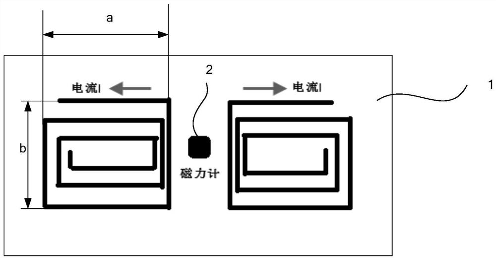
[0042] In order to facilitate the understanding of the anti-interference circuit board provided by the embodiment of the present application, its application scenario is firstly explained. The anti-interference circuit board is applied to terminals, such as common devices such as mobile phones, notebook computers, and tablet computers. The anti-interference circuit board is used to carry electronic devices, and the electronic devices are electronic devices that are easily disturbed by magnetic interference sources, such as magnetometers. When the magnetometer is used, it is very susceptible to some electromagnetic interference. For example, when the circuit on the anti-interference circuit board is working, the circuit will generate some interference magnetic fields, which li...


PUM


Abstract

The present application provides an anti-interference circuit board and a terminal. The circuit board specifically includes a substrate, the substrate has a first surface, and a first area for placing a magnetometer is provided on the first surface; A plurality of circuit layers, and a plurality of circuit layers are stacked, such as at least a stacked first functional circuit for generating a magnetic field generated in the first direction and a circuit for generating a magnetic field generated in the second direction are provided in the substrate The second functional circuit; when specifically setting the positions of the first functional circuit and the second functional circuit, it is satisfied that: the first area is located in the vertical projection of the first functional circuit and the second functional circuit on the first surface . It can be seen from the above description that the interference received by the magnetometer in the first area is compensated by setting the first functional circuit and the second functional circuit, and the first functional circuit and the second functional circuit are located below the magnetometer during setting, The surface area occupied by the anti-jamming circuit board is reduced.

Description

technical field [0001] The present application relates to the technical field of terminals, in particular to an anti-jamming circuit board and a terminal. Background technique [0002] The magnetic environment in the current mobile phone architecture scheme is relatively complicated. The layout of the magnetometer as a geomagnetic field detection device is limited in the whole machine environment. It is difficult to find a position with little magnetic interference on the PCB. It is necessary to use a PCB design hardware compensation solution to offset part of the magnetic field. interference. In the prior art, when compensating the magnetometer, such as figure 1 As shown in , the anti-jamming circuit board 1 is respectively provided with a coil 3 on both sides of the magnetometer 2 , and the magnetometer 2 is compensated by the coil 3 . However, when this method is adopted, a large area on the anti-jamming circuit board 1 is occupied, which reduces the places where other ...

Claims


Application Information

Patent Timeline
Patent Type & Authority Patents(China)
IPC IPC(8): H05K1/02H05K1/18H05K1/14
CPCH05K1/0228H05K1/18H05K1/144H05K2201/0979H05K2201/09663H05K2201/09672H05K2203/10H05K2201/09245H05K1/165H05K2201/10151H01F27/2804H01F2027/2809G01R33/0017G01R33/025H05K2201/093
Inventor 黄东
Owner HUAWEI TECH CO LTD
Why Eureka
Try Eureka