A kind of pcb board mounting equipment and mounting method

A PCB board and patch technology, which is applied in the field of PCB patch equipment and patch, patch equipment and patch, can solve problems such as PCB patch misalignment, electrical component misplacement, and electrical component offset, etc., to achieve Avoid misplacement, avoid accuracy, and reduce production time

Active Publication Date: 2021-05-14
宿州高科智能科技有限公司
View PDF8 Cites 0 Cited by
  • Summary
  • Abstract
  • Description
  • Claims
  • Application Information

AI Technical Summary

Problems solved by technology

[0003] The existing placement equipment and placement methods have the following deficiencies: (1) In the existing placement equipment, electrical components are pasted on the PCB by dispensing, and separate baking is required in the later stage. The electrical components are prone to offset; (2) The existing PCB board is prone to misalignment during placement, which makes the electrical components misplaced

Method used


Image

  • A kind of pcb board mounting equipment and mounting method
  • A kind of pcb board mounting equipment and mounting method
  • A kind of pcb board mounting equipment and mounting method

Examples


Embodiment Construction

[0031] In order to make the technical solutions of the present invention clearer and clearer to those skilled in the art, the present invention will be further described in detail below in conjunction with the examples and accompanying drawings, but the embodiments of the present invention are not limited thereto.

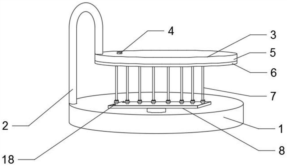
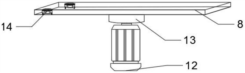
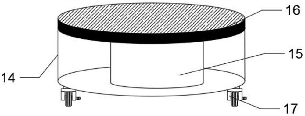
[0032] Such as Figure 1-Figure 8 As shown, the PCB board patching equipment provided in this embodiment includes a base 1 and a fourth motor 12 installed inside the base 1. The output end of the fourth motor 12 is connected to a patch plate 8 through a lifting rod 13, and the patch plate 8 is provided with a console 14, the top of the chip tray 8 is provided with a positioning plate 18, one side of the base 1 is provided with a rotating frame 2, and the other end of the rotating frame 2 is connected with a baking table 3, and the baking table 3 Inside is provided with material box 5, and the bottom of material box 5 is provided with motor box 6, and the inside of ...


PUM


Abstract

The invention discloses a PCB board patching device and a patching method, belonging to the technical field of PCB board patching, including a base and a fourth motor installed inside the base, the output end of the fourth motor is connected with a patch plate through a lifting rod , the interior of the patch plate is provided with a console, the top of the patch plate is provided with a positioning plate, one side of the base is provided with a rotating frame, the other end of the rotating frame is connected to a baking table, and the inside of the baking table is provided with a material box , the bottom of the material box is provided with a motor box, the inside of the material box is provided with a plurality of second motors, and the output ends of the second motors are connected with telescopic tubes. The present invention is provided with a baker to facilitate the baking of the electrical components after the patch is completed, ensuring the accuracy of the position of the components after baking to avoid displacement. At the same time, a baking lamp is provided to facilitate the PCB after the patch is completed. The board is baked as a whole, which is convenient to ensure the uniformity of the entire PCB board baking, without entering the baking oven for separate baking, reducing production time and improving production efficiency.

Description

technical field [0001] The invention relates to a patching device and a patching method, in particular to a PCB patching equipment and a patching method, belonging to the technical field of PCB patching. Background technique [0002] The placement machine is mainly used in the field of electronic product production. The placement machine is used to batch install some basic electronic components on the corresponding pads on the PCB. The main indicators to measure the performance of the placement machine are speed and accuracy. [0003] The existing placement equipment and placement methods have the following deficiencies: (1) In the existing placement equipment, electrical components are pasted on the PCB by dispensing, and separate baking is required in the later stage. The electrical components in the middle are prone to offset; (2) the existing PCB boards are prone to misalignment during patching, so that the electrical components are wrongly pasted. Contents of the inve...

Claims


Application Information

Patent Timeline
Patent Type & Authority Patents(China)
IPC IPC(8): H05K3/30H05K13/04H05K13/08
CPCH05K3/303H05K3/305H05K13/0469H05K13/0406H05K13/081
Inventor 张严马开静张冬冬王秀梅蒲生星
Owner 宿州高科智能科技有限公司
Why Eureka
Try Eureka