High-frequency front-end circuit
一种前端电路、高频的技术,应用在高频前端电路领域,能够解决功率放大器振荡等问题,达到抑制输出特性的劣化的效果
- Summary
- Abstract
- Description
- Claims
- Application Information
AI Technical Summary
Problems solved by technology
Method used
Image

Examples
Embodiment approach 1
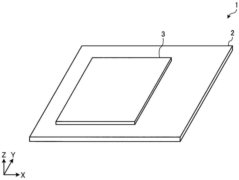
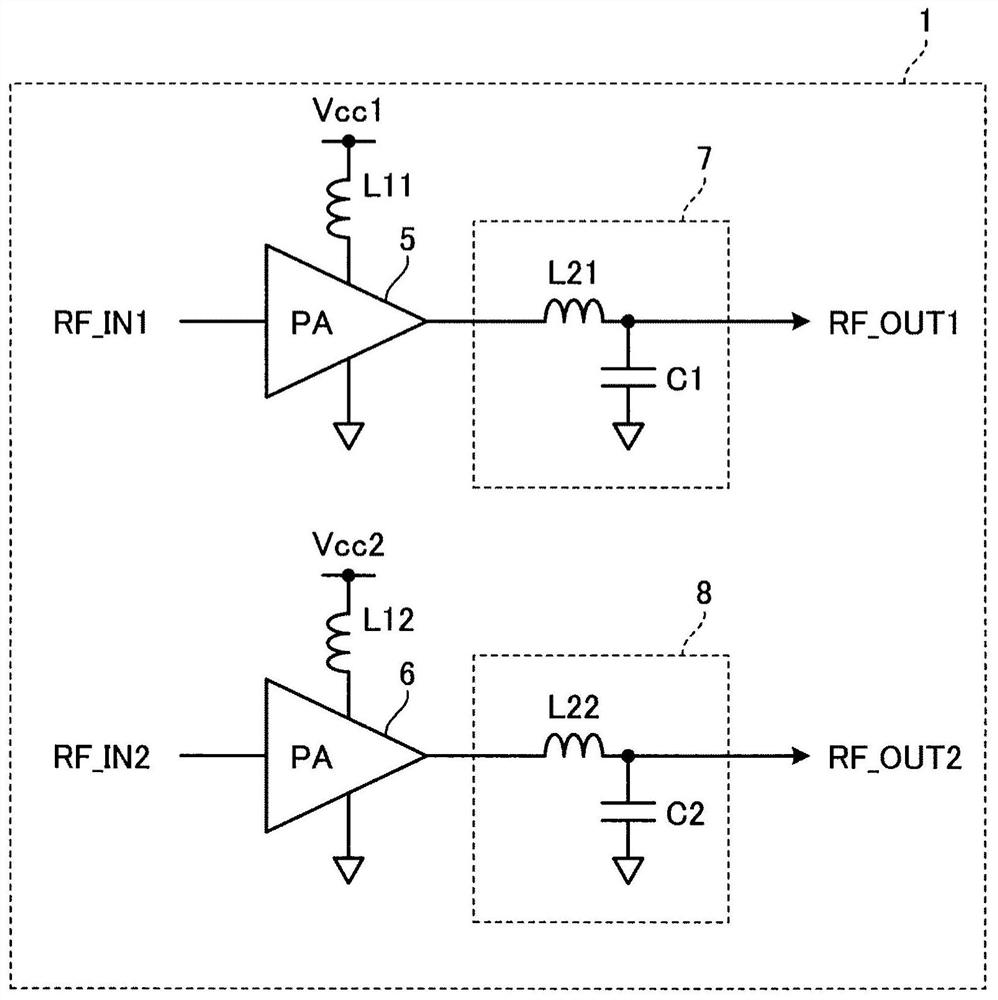
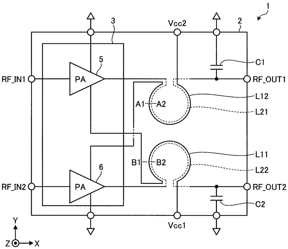
[0038] figure 1 It is a diagram showing the appearance of the high-frequency front-end circuit according to the first embodiment. A high-frequency front-end circuit 1 according to Embodiment 1 includes a substrate 2 and a substrate 3 .
[0039] The high-frequency front-end circuit 1 can be used in mobile wireless communication terminal devices such as mobile phones and smart phones to transmit and receive various signals such as voice and data to and from a base station.
[0040] The substrate 2 is a non-semiconductor substrate. As for the substrate 2 , a rigid substrate made of glass epoxy resin, LTCC (Low Temperature Co-fired Ceramic, low temperature co-fired ceramic), etc., or a flexible substrate made of liquid crystal polymer, polyimide resin, or the like can be exemplified.
[0041] The substrate 3 is a semiconductor substrate. An IC (Integrated Circuit, integrated circuit) chip (die) can be illustrated as the substrate 3 .
[0042] The substrate 2 is parallel to the...
Embodiment approach 2
[0065] Figure 5 It is a diagram showing a schematic configuration of a high-frequency front-end circuit according to Embodiment 2. In addition, the same reference numerals are assigned to the same components as those in Embodiment 1, and description thereof will be omitted.
[0066] In this embodiment, the first power amplifier 5, the second power amplifier 6, the first power supply inductor L11, the second power supply inductor L12, the first matching inductor L21, and the second The matching inductor L22 is provided on the substrate 3a.
[0067] In this embodiment, the substrate 3 a is a semiconductor substrate and constitutes an IC chip arranged on the substrate 2 . Contains the first power amplifier 5, the second power amplifier 6, the first power supply inductor L11, the second power supply inductor L12, the first matching inductor L21, and the second matching inductor The IC chip of L22 is mounted on a substrate 2 which is a non-semiconductor substrate, and constitut...
Embodiment approach 3
[0073] Figure 6 It is a diagram showing the appearance of the high-frequency front-end circuit according to Embodiment 3. Figure 7 It is a diagram showing a schematic configuration of a high-frequency front-end circuit according to Embodiment 3. In addition, the same reference numerals are assigned to the same components as those in Embodiments 1 and 2, and description thereof will be omitted.
[0074] A high-frequency front-end circuit 1 b according to Embodiment 3 includes a substrate 2 , a substrate 3 , and a substrate 4 .
[0075] The substrate 4 is a semiconductor substrate. As for the substrate 4 , an integrated passive device (IPD; Integrated Passive Device, integrated passive device) can be exemplified.
[0076] The substrate 4 is parallel to the X-Y plane. Moreover, the board|substrate 4 and the board|substrate 2 are arrange|positioned overlapping, seeing from Z direction. The substrate 2 has an area equal to or larger than a region where the substrate 3 and th...
PUM
 Abstract
Description
Claims
Application Information
 - R&D
- Intellectual Property
- Life Sciences
- Materials
- Tech Scout
- Unparalleled Data Quality
- Higher Quality Content
- 60% Fewer Hallucinations
Browse by: Latest US Patents, China's latest patents, Technical Efficacy Thesaurus, Application Domain, Technology Topic, Popular Technical Reports.
© 2025 PatSnap. All rights reserved.Legal|Privacy policy|Modern Slavery Act Transparency Statement|Sitemap|About US| Contact US: help@patsnap.com