Adapter plate facilitating underfill of large-size element and manufacturing method thereof

An underfill and transfer board technology, used in semiconductor/solid-state device manufacturing, electrical components, semiconductor/solid-state device components, etc., can solve the problems of underfilling, product failure, and insufficient filling of plastic packaging materials, and increase the bottom Height, increase the filling space, and ensure the effect of product reliability

Pending Publication Date: 2020-09-08
JCET GROUP CO LTD
View PDF0 Cites 0 Cited by
  • Summary
  • Abstract
  • Description
  • Claims
  • Application Information

AI Technical Summary

Problems solved by technology

[0002] At present, some large SIP products are directly surface-mounted with relatively large-sized QFN or LGA products and directly filled with plastic encapsulants. However, the bottom spacing of these products is generally less than 50um after surface-mounting, and it is difficult for the plastic encapsulant to completely fill the bottom. , there will be insufficient filling problems, resulting in failure of subsequent products

Method used


Image

  • Adapter plate facilitating underfill of large-size element and manufacturing method thereof
  • Adapter plate facilitating underfill of large-size element and manufacturing method thereof
  • Adapter plate facilitating underfill of large-size element and manufacturing method thereof

Examples


Embodiment Construction

[0026] The present invention will be further described in detail below in conjunction with the accompanying drawings and embodiments.

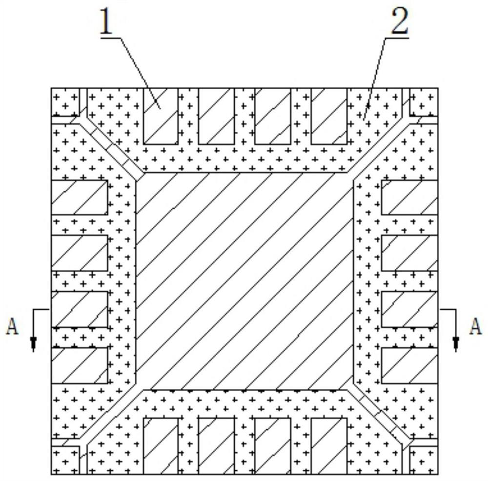
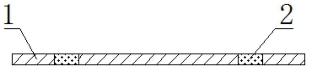
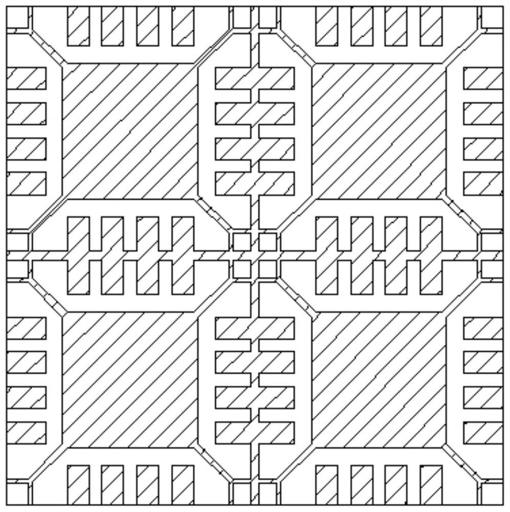
[0027] see figure 1 , figure 2 , the present invention relates to an adapter board that is easy to fill the bottom of large-sized components, which includes a copper column layer 1, the pattern of the copper column layer 1 corresponds to the pattern of the bottom pad of the mounted component, and the copper column layer 1 A dielectric material 2 is arranged between them, and the dielectric material 2 is a photosensitive material whose solubility will change after being illuminated.

[0028] The photosensitive material is a quinone azido compound material, which undergoes a photodecomposition reaction after being irradiated, and can change from oil solubility to water solubility.

[0029] The size of the adapter board is the same as the size of the mounted components.

[0030] Its manufacturing method comprises the following steps:

[0031...


PUM


Abstract

The invention relates to an adapter plate facilitating underfill of a large-size element and a manufacturing method thereof. The adapter plate comprises a copper column layer (1), the pattern of the copper column layer (1) corresponds to the pattern of a welding pad at the bottom of a subsequent mounting element, the periphery of the copper column layer (1) is encapsulated with a dielectric material (2), the dielectric material (2) is made of a photosensitive material, and the solubility of the photosensitive material can change after the photosensitive material is illuminated. According to the adapter plate easy to fill the bottom of the large-size element and the manufacturing method thereof, the gap at the bottom of the surface mounting device can be raised, so that the plastic packagematerial is easier to fill.

Description

technical field [0001] The invention relates to an adapter board which is easy to fill the bottom of large-size components and a manufacturing method thereof, belonging to the technical field of semiconductor packaging. Background technique [0002] At present, some large SIP products are directly surface-mounted with relatively large-sized QFN or LGA products and directly filled with plastic encapsulants. However, the bottom spacing of these products is generally less than 50um after surface-mounting, and it is difficult for the plastic encapsulant to completely fill the bottom. , there will be insufficient filling problems, resulting in failure of subsequent products. Contents of the invention [0003] The technical problem to be solved by the present invention is to provide an adapter board that is easy to fill the bottom of large-sized components and its manufacturing method in view of the above-mentioned prior art. filling. [0004] The technical solution adopted by...

Claims


Application Information

Patent Timeline
IPC IPC(8): H01L23/498H01L21/48H01L21/60
CPCH01L23/49816H01L23/49838H01L21/4853H01L24/81H01L2224/81345Y02P70/50
Inventor 李全兵顾骁宋健
Owner JCET GROUP CO LTD
Why Eureka
Try Eureka