Delay overcurrent protection circuit and design method thereof

A design method and overcurrent technology, applied in emergency protection circuit devices, circuit devices, emergency protection devices with automatic disconnection, etc., can solve problems such as inconvenient use, achieve wide application prospects, simple structure, and reliable design principles Effect

Active Publication Date: 2020-09-25
SUZHOU LANGCHAO INTELLIGENT TECH CO LTD
View PDF4 Cites 1 Cited by
  • Summary
  • Abstract
  • Description
  • Claims
  • Application Information

AI Technical Summary

Problems solved by technology

[0004] If the output is a dynamic load or needs to increase the output current in a short period of time, it will

Method used


Image

  • Delay overcurrent protection circuit and design method thereof
  • Delay overcurrent protection circuit and design method thereof
  • Delay overcurrent protection circuit and design method thereof

Examples


Embodiment 1

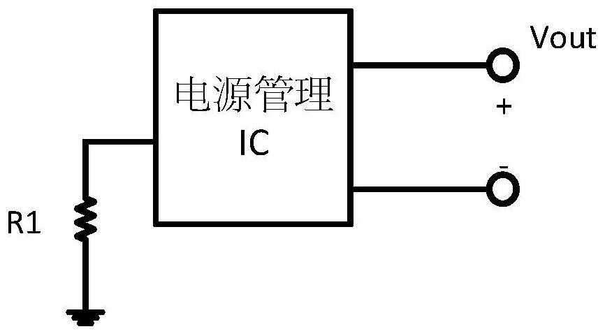
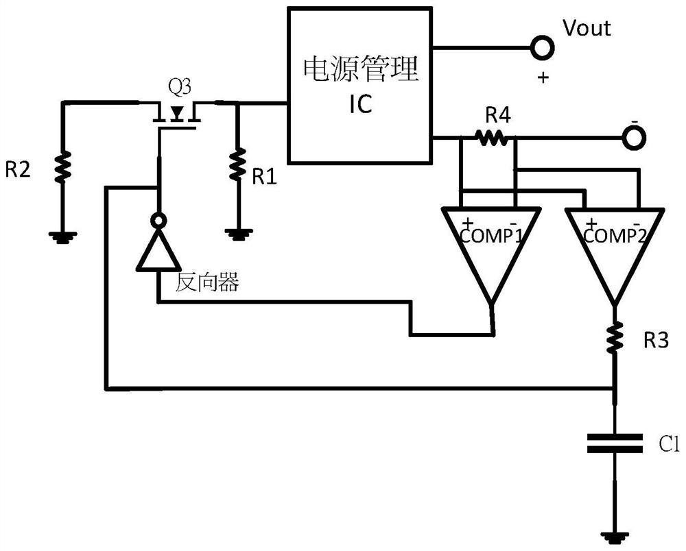
[0035] Such as image 3 As shown, this embodiment provides a delayed overcurrent protection circuit, including a power management IC and a loop connected outside the power management IC; the loop includes: a first protection resistor R1, a second protection resistor R2, n Channel MOS transistor Q3, low-impedance resistor R, second comparator COMP2, third protection resistor R3, capacitor C1, inverter, and first comparator COMP1; the first protection resistor R1 and the n-channel MOS transistor Q3 The D poles of the power management IC are respectively connected to the power management IC, and the second protection resistor R2 is connected to the S pole of the n-channel MOS transistor Q3; the negative pole of the output terminal of the power management IC is connected in series with a low-impedance resistor R4; the input of the first comparator COMP1 terminal and the input terminal of the second comparator COMP2 are respectively connected in parallel at both ends of the low-imp...

Embodiment 2

[0043] This embodiment provides a design method for delayed overcurrent protection, and the main body of the design method may be a circuit for delayed overcurrent protection.

[0044] Specifically, the design method of a delayed overcurrent protection includes:

[0045] S1, add n-channel MOS transistor Q3 and the second protection resistor R2 connected in parallel with the first protection resistor R1, and set the n-channel MOS transistor Q3 to be in the on state during initialization, which is used to reduce the overcurrent protection point in the normal working state. When increasing the overcurrent protection point in the subsequent steps, in order not to affect the overcurrent protection mechanism and keep the subsequent overcurrent protection point as it is, it is necessary to reduce the overcurrent protection point first;

[0046] S2, increase the low-impedance resistor R4, the first comparator COMP1 and the inverter, set the first comparator COMP1 to monitor the voltag...


PUM


Abstract

The invention provides a delay overcurrent protection circuit and a design method thereof. The delay overcurrent protection circuit comprises a power supply management IC and a loop connected to the exterior of the power supply management IC, and the loop comprises a first protection resistor R1, a second protection resistor R2, an n-channel MOS tube Q3, a charging time-delay circuit and a comparison circuit. The first protection resistor R1 and the D pole of the n-channel MOS tube Q3 are respectively connected with the power supply management IC, and the second protection resistor R2 is connected with the S pole of the n-channel MOS tube Q3; the G electrode of the n-channel MOS tube Q3 is connected with the output end of the comparison circuit, the input end of the charging time-delay circuit and the input end of the comparison circuit are separately connected with the negative electrode of the output end of the power supply management IC, and the first protective resistor R1, the second protective resistor R2 and the charging delay circuit are all grounded. According to the invention, the overcurrent protection is delayed for the condition that the overcurrent protection mechanism is triggered by instantaneously increasing the output current, so that the convenience in use of the power supply management IC is improved.

Description

technical field [0001] The invention belongs to the technical field of power supply safety, and in particular relates to a delayed overcurrent protection circuit and a design method. Background technique [0002] Usually, the overcurrent protection method of power management IC is to adjust the size of the overcurrent protection by changing the resistance outside the IC. The larger the resistance, the larger the overcurrent protection point, and the smaller the resistance, the larger the overcurrent protection point. Small; [0003] Existing power management ICs set the way of over-current protection as follows: figure 1 As shown, the current protection is realized by connecting a protection resistor externally. Such as figure 2 As shown, a comparator is set inside the power management IC. After the current source at the negative terminal of the comparator flows through the protection resistor, a reference voltage V- is generated; the positive terminal of the comparator ...

Claims


Application Information

Patent Timeline
IPC IPC(8): H02H3/093H02H7/10
CPCH02H3/093H02H7/10
Inventor 杨益昌
Owner SUZHOU LANGCHAO INTELLIGENT TECH CO LTD
Why Eureka
Try Eureka