Time of flight sensor device and time of flight sensor arrangement

A sensor device, time-of-flight technology, applied in the field of integrated circuits and optical sensor devices, can solve the problems of inability to obtain signal-to-noise ratio and high temperature operability

Pending Publication Date: 2020-09-29
INFINEON TECH AG
View PDF0 Cites 0 Cited by
  • Summary
  • Abstract
  • Description
  • Claims
  • Application Information

AI Technical Summary

Problems solved by technology

[0003] However, existing designs of optical time-of-flight sensor devices are limited by the sensor signal quality (i.e., in the transfer efficiency of the photogenerated charge to the readout node(s), cannot achieve good signal-to-noise ratio and high temperature reliability. Operability (i.e., in terms of transfer efficiency of photogenerated charge to the readout node(s))

Method used


Image

  • Time of flight sensor device and time of flight sensor arrangement
  • Time of flight sensor device and time of flight sensor arrangement
  • Time of flight sensor device and time of flight sensor arrangement

Examples


Embodiment Construction

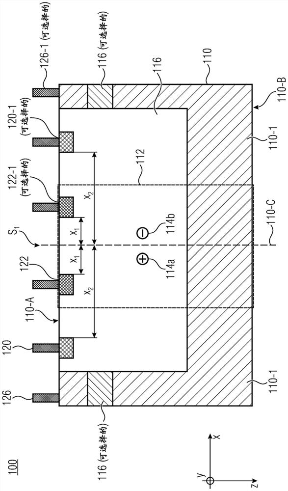
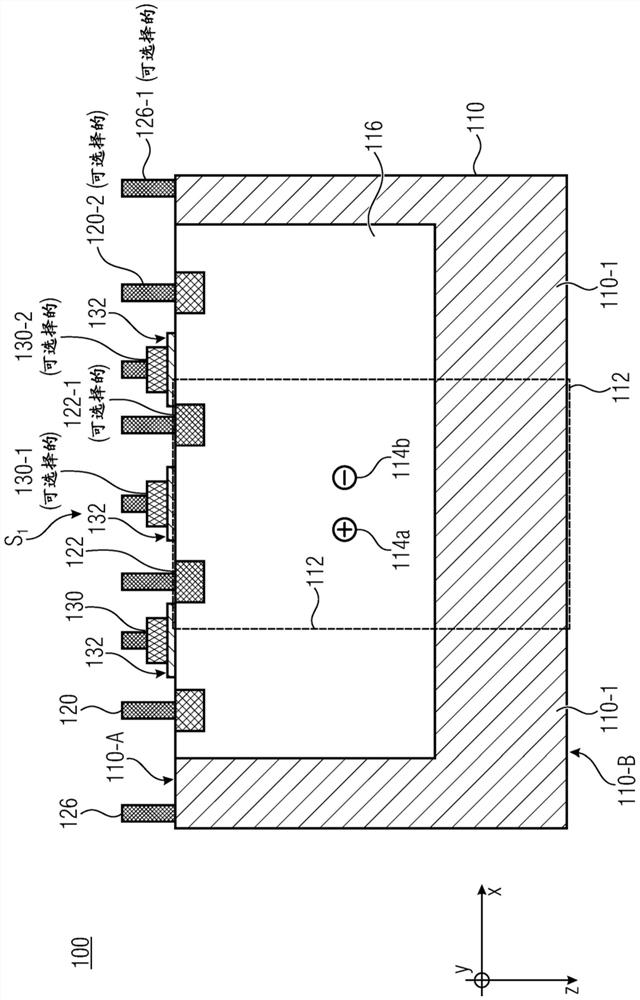
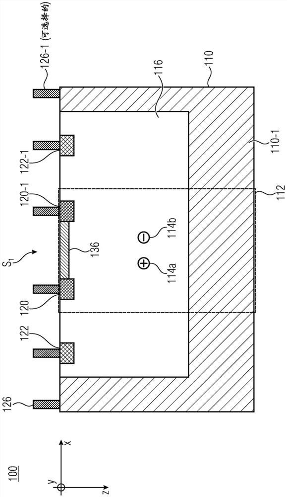
[0023] In the following description, embodiments are discussed in detail, however it should be appreciated that the embodiments provide many applicable concepts that can be implemented in a wide variety of semiconductor devices. The specific embodiments discussed are merely illustrative of specific ways to make and use the concepts, and do not limit the scope of the embodiments. In the description of the following embodiments, the same or similar elements having the same function have the same reference numerals or the same names, and descriptions of such elements will not be repeated in each embodiment. Also, the features of the different embodiments described below may be combined with each other unless specifically stated otherwise.

[0024] It will be understood that when an element is referred to as being "connected" or "coupled" to another element, it can be directly connected or coupled to the other element or intervening elements may be present. In contrast, when an e...


PUM

PropertyMeasurementUnit
thicknessaaaaaaaaaa

Abstract

The disclosure relates to a time of flight sensor device and a time of flight sensor arrangement. According to an embodiment, The time of flight sensor device comprises: a semiconductor substrate comprising a conversion region to convert an electromagnetic signal in photo-generated charge carriers, and comprising a substrate doping region having a n doping type, wherein the substrate doping regionextends from a first main surface region of the semiconductor substrate into the semiconductor substrate, wherein the semiconductor substrate has adjacent to the substrate doping region doped region,and wherein the substrate doping region at least partially forms the conversion region in the semiconductor substrate, a readout node arranged in the semiconductor substrate within the substrate doping region and having the n-doping type, wherein the readout node is configured to readout the photo generated charge carriers; and a control electrode arranged in the substrate doping region of the semiconductor substrate and in the substrate doping region and having the p-doping type.

Description

technical field [0001] Embodiments relate generally to the field of integrated circuits, and more particularly, to the field of optical sensor devices adapted to detect time-of-flight of electromagnetic signals. Accordingly, embodiments relate to time-of-flight (TOF) sensor devices. Other embodiments relate to N-epi time-of-flight sensor devices having an n-doped semiconductor region in a semiconductor substrate (eg, a bulk or epitaxially grown semiconductor substrate). Background technique [0002] Existing optical time-of-flight sensors employ a photogate structure for redirecting photogenerated charge carriers in a semiconductor substrate to a readout node for obtaining time-of-flight information of an amplitude-modulated electromagnetic signal generated by a radiation source, Wherein the electromagnetic signal is directed to the object and reflected to the time-of-flight sensor device. [0003] However, existing designs of optical time-of-flight sensor devices are limi...

Claims


Application Information

Patent Timeline
Patent Type & Authority Applications(China)
IPC IPC(8): H01L27/146
CPCH01L27/14601H01L27/14605H01L27/14609G01S7/4914G01S17/894H01L27/1443H01L31/02019H01L31/0224H01L31/103
Inventor H·菲克
Owner INFINEON TECH AG
Why Eureka
Try Eureka