High-resolution full-color Micro LED display

A high-resolution, full-color technology, applied in the direction of electric solid-state devices, semiconductor devices, electrical components, etc., can solve the problem that the secondary optical regulation function of the reflective cup cannot be brought into play, achieve high secondary optical regulation, and overcome optical crosstalk , Solve the effect of optical crosstalk

Active Publication Date: 2020-09-29
深圳市惠合显示有限公司
View PDF16 Cites 18 Cited by
  • Summary
  • Abstract
  • Description
  • Claims
  • Application Information

AI Technical Summary

Problems solved by technology

Its main disadvantage is that when the light emitted by the MicroLED chip passes through the fluorescent material layer for wavelength conversion, the light will be scattered by the fluorescent material layer, so that the secondary optical regulation function of the reflective cup cannot be exerted.

Method used


Image

  • High-resolution full-color Micro LED display
  • High-resolution full-color Micro LED display
  • High-resolution full-color Micro LED display

Examples


Embodiment 1

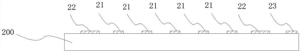
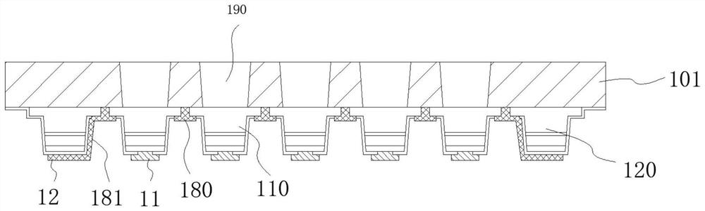
[0058] Please refer to Figure 1 to Figure 6 , a high-resolution full-color MicroLED display, provided with a driving substrate 200, a MicroLED array module 100, the surface on the driving substrate 200 is provided with a first pad 21 and a second pad 22, the lower surface of the MicroLED array module 100 The first electrode 11 and the second electrode 12 are provided, and the lower surface of the MicroLED array module 100 is welded face-to-face with the upper surface of the driving substrate 200, so that the first electrode 11 and the first pad 21 are welded together, and the second electrode 12 Solder with the second pad 22 together.

[0059] The MicroLED array module 100 is provided with MicroLED light-emitting chips 110 and dummy chips 120, and there are several MicroLED light-emitting chips 110, and each MicroLED light-emitting chip 110 is provided with a first electrode 11 on the lower surface, and the second electrode 12 is provided with on the lower surface of the dum...

Embodiment 2

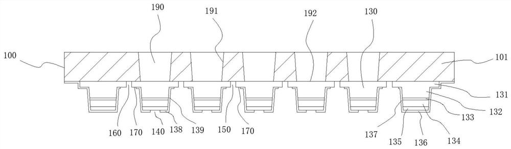
[0083] Please refer to Figure 7 The MicroLED array module 100 is provided with a MicroLED light-emitting chip 110 and a dummy chip 120. There are several MicroLED light-emitting chips 110. A first electrode 11 is provided on the lower surface of each MicroLED light-emitting chip 110. The second electrode 12 It is disposed on the lower surface of the dummy chip 120 . The plurality of Micro LED light-emitting chips 110 are distributed into an array according to a fixed pitch between rows and columns.

[0084] The dummy chips 120 are also provided with several pieces, each dummy chip 120 is provided with a second electrode 12 on the lower surface, and the size of the dummy chips 120 is equal to the size of the MicroLED light-emitting chip 110 . The dummy chip 120 is independent from the dummy chip 120 . The row spacing of the dummy chips 120 is equal to the row spacing of the array of Micro LED light-emitting chips 110 .

[0085] The dummy chips 120 surround the periphery of ...

Embodiment 3

[0088] Please refer to Figure 8 The dummy chips 120 are also provided with several pieces, and the lower surface of each dummy chip 120 is provided with two first electrodes 11 , and the size of the dummy chips 120 is equal to the size of the MicroLED light-emitting chip 110 . The dummy chip 120 is independent from the dummy chip 120 . The row spacing and column spacing of the dummy chips 120 are respectively equal to the row spacing and column spacing of the array of Micro LED light-emitting chips 110 .

[0089] The dummy chip 120 is disposed on the periphery of the array of Micro LED light-emitting chips 110 . The MicroLED array module 100 is square, and the dummy chips 120 are distributed on two of the four outer sides of the MicroLED array module 100 .

[0090] All the other are identical with embodiment two.


PUM

PropertyMeasurementUnit
wavelengthaaaaaaaaaa

Abstract

The invention relates to a high-resolution full-color Micro LED (Light Emitting Diode) display. A Micro LED light-emitting chip and a dummy chip are arranged on the display, wherein the MicroLED light-emitting chip and the dummy chip are respectively provided with a first semiconductor layer and an insulating layer, the insulating layer coats side walls of the MicroLED light-emitting chip and thedummy chip, a first spacing groove is formed between step parts of first semiconductor layers of the adjacent MicroLED light-emitting chips, a second spacing groove is formed between the first semiconductor layer step part of the MicroLED light-emitting chip and the first semiconductor layer step part of the adjacent dummy chip, part of a lower surface of the step part of the first semiconductor layer is not covered by the insulating layer, and metal circuits are arranged in the first spacing groove, the second spacing groove and the lower surface, not covered by the insulating layer, of the step part of the first semiconductor layer.

Description

technical field [0001] The invention relates to the field of novel displays, in particular to a high-resolution full-color MicroLED display. Background technique [0002] Micro LED display is a new next-generation display technology after liquid crystal display and OLED display. Micro LED displays use LED light-emitting chips (Micro LED chips) with a size ranging from a few microns to tens of microns as pixel units, which are closely arranged in an array, and each chip can be independently driven to light up and emit light. Micro LED display will also be an important development direction for the cross-border integration of the two major industries of new display and LED. It will realize the horizontal integration of display, semiconductor, integrated circuit and other industries. Micro LED displays have many advantages such as self-illumination, high efficiency, long life, and ultra-high resolution. The application products displayed by Micro LED are expected to cover all...

Claims


Application Information

Patent Timeline
Patent Type & Authority Applications(China)
IPC IPC(8): H01L27/15H01L33/48H01L33/50H01L33/60H01L33/62
CPCH01L27/156H01L33/486H01L33/60H01L33/507H01L33/62
Inventor 郭伟杰
Owner 深圳市惠合显示有限公司
Why Eureka
Try Eureka