Semiconductor device and forming method thereof

A technology of semiconductors and devices, applied in the field of semiconductor devices and their formation, can solve the problem that the surface uniformity and shape of fins cannot be well controlled

Pending Publication Date: 2020-10-09
SEMICON MFG INT (SHANGHAI) CORP +1
View PDF0 Cites 0 Cited by
  • Summary
  • Abstract
  • Description
  • Claims
  • Application Information

AI Technical Summary

Problems solved by technology

[0006] The purpose of the present invention is to provide a semiconductor device and its forming method, which solves the problem that t

Method used


Image

  • Semiconductor device and forming method thereof
  • Semiconductor device and forming method thereof
  • Semiconductor device and forming method thereof

Examples


Embodiment Construction

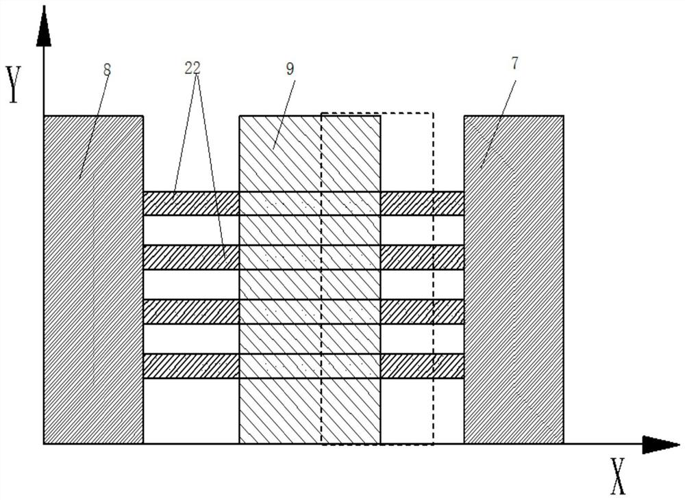
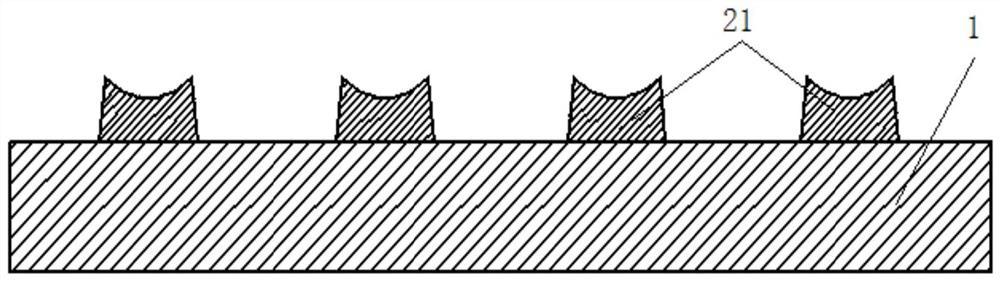
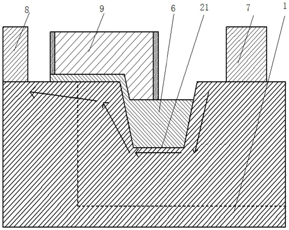
[0041] The following is a clear and complete description of the technical solutions of the present invention through the accompanying drawings. Apparently, the described embodiments are part of the embodiments of the present invention, not all of them. Based on the embodiments of the present invention, all other embodiments obtained by persons of ordinary skill in the art without making creative efforts belong to the protection scope of the present invention.

[0042] In the description of the present invention, it should be noted that the terms "center", "upper", "lower", "left", "right", "vertical", "horizontal", "inner", "outer" etc. The indicated orientation or positional relationship is based on the orientation or positional relationship shown in the drawings, and is only for the convenience of describing the present invention and simplifying the description, not to indicate or imply that the referred device or element must have a specific orientation, use a specific Azim...


PUM


Abstract

The invention provides a semiconductor device and a forming method thereof, and the method comprises the following steps: providing a substrate, and forming a first sub-fin part after removing a partof fin parts in thickness on the substrate; adjusting the end, away from the substrate, of the first sub-fin part to enable S1 to be greater than or equal to S2, wherein S1 is the distance from the middle area of the end face of one end of the first sub-fin part to the substrate, and S2 is the distance from the edge area of the end face of the first sub-fin part to the substrate, and in a cross section formed perpendicular to the length direction of the first sub-fin part, the contour line of one side, far away from the substrate, of the first sub-fin part is in smooth transition. The semiconductor device is manufactured through the forming method of the semiconductor device. The distance from the middle area of the end face of one end of the first sub-fin part to the substrate is greaterthan or equal to the distance from the edge area of the first sub-fin part to the substrate, the contour line of the side, away from the substrate, of the first sub-fin part is in smooth transition, the probability that the bottom area of the first sub-fin part is broken down by voltage can be reduced, and therefore the performance of the semiconductor device is optimized.

Description

technical field [0001] The invention relates to the technical field of semiconductors, in particular to a semiconductor device and a forming method thereof. Background technique [0002] With the development of integrated circuits to ultra-large-scale integrated circuits, the circuit density inside the integrated circuit is increasing, and the number of components contained in the integrated circuit is also increasing, and the size of the components is also reduced. In order to further reduce the size of semiconductor devices, fin field effect transistors have been developed. The fin field effect transistor is a three-dimensional structure, and one or more protruding fins are formed on the fin field effect transistor, insulating isolation parts are arranged between the fins, and the gate spans the fins and covers the top and side walls of the fins . [0003] LDMOS (Laterally Diffused Metal Oxide Semiconductor) is an important part of FinFET (Fin Field Effect Transistor), i...

Claims


Application Information

Patent Timeline
IPC IPC(8): H01L29/78H01L21/336H01L29/06
CPCH01L29/0657H01L29/66681H01L29/66795H01L29/7816H01L29/7853
Inventor 王楠
Owner SEMICON MFG INT (SHANGHAI) CORP
Why Eureka
Try Eureka