Manufacturing process of printed circuit board with steps and printed circuit board

A technology of printed circuit board and manufacturing process, which is applied in the direction of printed circuit manufacturing, printed circuit, and secondary treatment of printed circuit, etc. It can solve the problems that the graphics transfer cannot be completed, and the dry film cannot be tightly attached to the protruding or concave position.

Inactive Publication Date: 2020-10-13
珠海杰赛科技有限公司 +1
View PDF3 Cites 3 Cited by
  • Summary
  • Abstract
  • Description
  • Claims
  • Application Information

AI Technical Summary

Problems solved by technology

Subsequently, higher requirements have been put forward for production and manufacturing. Conventional printed circuit board pattern transfer is realized on a flat surface through special dry film, but for printed circuit boards designed with steps (cavities), dry film It is impossible to stick tightly on the protruding or concave position, and it is impossible to complete the graphic transfer on the outer layer of the copper clad laminate at one time. The inner layer of the graphic at the bottom of the step is etched out first, and then laminated, or the bottom of the step only supports full metal retention. (or not to keep) the only choice, when designing steps with multiple depths, the side walls of the steps are covered with metal and the bottom has different electrical patterns, the traditional process cannot complete the pattern transfer at the bottom of the steps, so it is necessary to study the ability to complete the surface layer at one time and the technology of graphic transfer at the bottom of the steps

Method used


Image

  • Manufacturing process of printed circuit board with steps and printed circuit board

Examples


Embodiment Construction

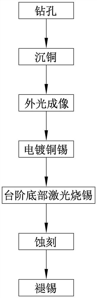
[0018] Embodiments of the present invention are described in detail below, examples of which are shown in the drawings, wherein the same or similar reference numerals designate the same or similar elements or elements having the same or similar functions throughout. The embodiments described below by referring to the figures are exemplary only for explaining the present invention and should not be construed as limiting the present invention.

[0019] In the description of the present invention, it should be understood that if there is a description related to orientation, such as the orientation or positional relationship indicated by up, down, front, back, left, right, etc., the orientation description can be based on the orientation shown in the accompanying drawings. Orientation or positional relationship is only for the convenience of describing the present invention and simplifying the description, and does not indicate or imply that the referred device or element must hav...


PUM


Abstract

The invention discloses a manufacturing process of a printed circuit board with a step, which comprises the following steps: external light imaging: manufacturing a circuit pattern on a copper-clad plate in a dry film pasting mode, designing a dry film removal effect at the step position, and exposing copper on the side wall and the bottom of the step; electroplating copper and tin: sequentially electroplating a copper layer and a tin layer on the circuit pattern area on the copper-clad plate; step bottom laser tin burning: exposing the electrocoppering layer at the bottom of the step by meansof laser ablation of the tin layer; etching: after the dry film on the copper-clad plate is removed, etching off the exposed copper layer on the copper-clad plate to obtain the copper-clad plate of which the circuit pattern is covered by the tin layer; and tin removing: removing the tin layer on the copper-clad plate to obtain the printed circuit board with the outer layer circuit. According to the technological method, the technological process is shortened, and the manufacturing speed is increased. The invention further discloses a printed circuit board manufactured by adopting the manufacturing process. The printed circuit board is provided with a step mechanism.

Description

technical field [0001] The invention relates to the technical field of printed circuit boards, in particular to a manufacturing process of a stepped printed circuit board and the printed circuit board. Background technique [0002] As the large-scale design of the high-end PCB market accelerates towards high-frequency and high-speed design, printed circuit boards designed with steps (cavities) can greatly improve the heat dissipation of components, and printed circuit boards can achieve better shielding effects, and printed circuit boards The volume of the circuit board can be made smaller. Subsequently, higher requirements have been put forward for production and manufacturing. Conventional printed circuit board pattern transfer is realized on a flat surface through special dry film, but for printed circuit boards designed with steps (cavities), dry film It is impossible to stick tightly on the protruding or concave position, and it is impossible to complete the graphic tr...

Claims


Application Information

Patent Timeline
Patent Type & Authority Applications(China)
IPC IPC(8): H05K3/02H05K3/06H05K3/18H05K3/28
CPCH05K3/027H05K3/06H05K3/18H05K3/282H05K2203/052H05K2203/107
Inventor 邓勇刘国汉李静周德良
Owner 珠海杰赛科技有限公司
Why Eureka
Try Eureka