A kind of sic MPS diode device and preparation method thereof

A diode and device technology, applied in the field of SiCMPS diode devices and their preparation, can solve the problems of forward current rebound, device forward function degradation, etc., and achieves the improvement of surge capability, suppression of rapid return of voltage drop, and improvement of injection efficiency. Effect

Active Publication Date: 2021-09-24
XIDIAN UNIV
View PDF0 Cites 0 Cited by
  • Summary
  • Abstract
  • Description
  • Claims
  • Application Information

AI Technical Summary

Problems solved by technology

[0004] Problems with SiC MPS diode devices: The current SiC MPS diodes will have a forward current rebound phenomenon when turned on, which is called "snapback", and bipolar degradation will cause the forward function of the device to degrade

Method used


Image

  • A kind of sic MPS diode device and preparation method thereof
  • A kind of sic MPS diode device and preparation method thereof
  • A kind of sic MPS diode device and preparation method thereof

Examples


preparation example Construction

[0032] The preparation method of the above-mentioned SiC MPS diode device comprises the following steps:

[0033] S1: An N- epitaxial layer 4 is formed by epitaxial growth on the N+ substrate 5; the overall structure forming the N- epitaxial layer is usually called an epitaxial wafer;

[0034] S2: Preparation of SiO on N-epitaxial layer 4 2 The mask layer is formed with a mask pattern by a photolithography process, and an N+ implantation region 3 is formed by means of N ion implantation;

[0035] S3: cleaning off the implantation mask layer, forming a new mask layer on the surface, forming a mask pattern by photolithography, and forming a P+ implantation region 2 by means of Al ion implantation;

[0036] S4: cleaning off the implanted mask layer, forming a new mask layer on the surface, forming a mask pattern by photolithography, and then forming a trench structure 7 by ICP etching;

[0037] S5: Protect the surface of the epitaxial layer with a carbon film, activate the impl...

Embodiment 1

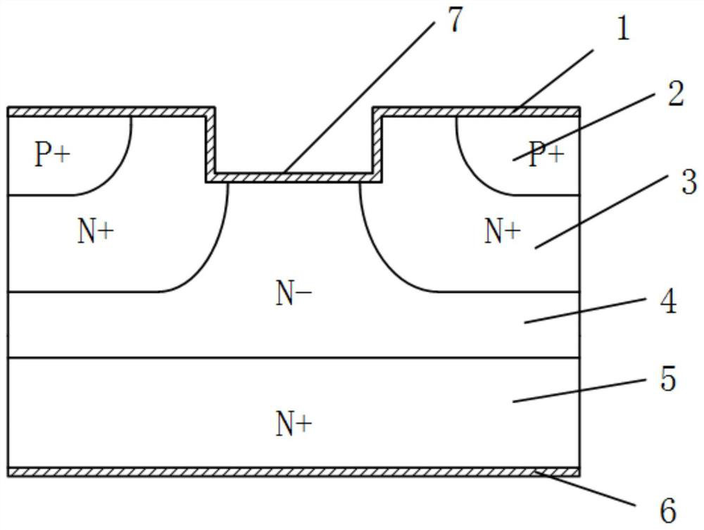
[0043] figure 1 A schematic cross-sectional view of a trench type SiCMPS diode device structure that has carried out N+ implantation for the present invention, combined below figure 1 Describe in detail the apparatus of the present invention;

[0044] A trench-type SiC MPS diode device structure with N+ implantation: including an N+ substrate 5 with a doping concentration of 5×10 18 atom / cm 3 Made of SiC material with a thickness of 350 μm, the lightly doped N- epitaxial layer 4 is located on the N+ substrate 5; the cathode 6 is located below the substrate; the surface of the N- epitaxial layer 4 is provided with a trench structure 7; the P+ implantation region 2 is located The surface of the N- epitaxial layer 4 around the trench structure 7; the N+ implantation region 3 is located around the P+ implantation region 2, and the anode covers the entire surface of the P+ implantation region 2 and the surface of the trench structure 7.

[0045] The process steps are as follows:...

Embodiment 2

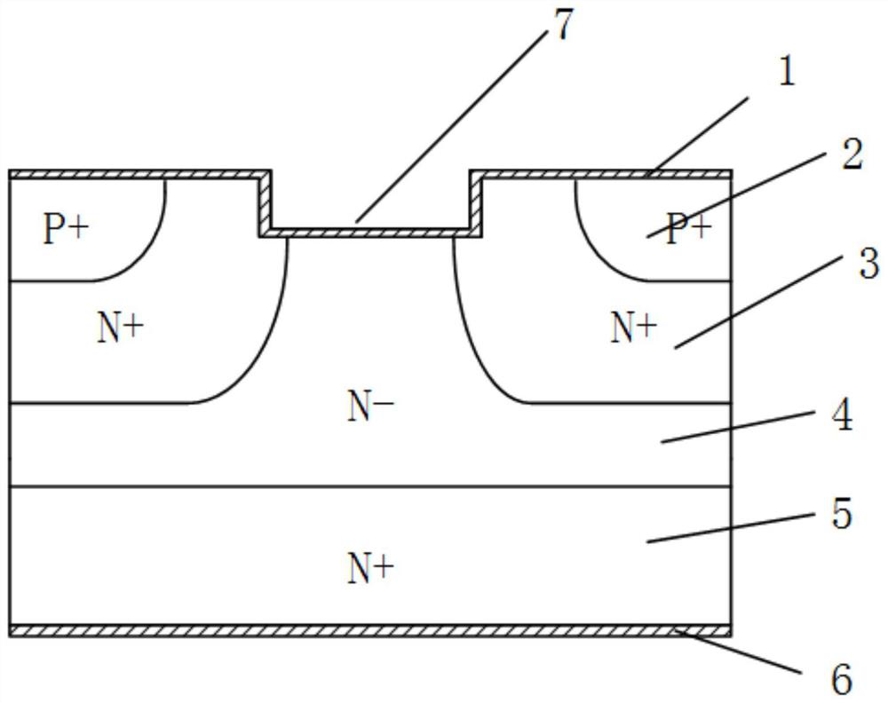
[0055] figure 2 It is a schematic cross-sectional view of the structure of a trench type SiC MPS diode device with N+ implantation in the present invention, combined below figure 2 Describe in detail the apparatus of the present invention;

[0056] A trench type SiC MPS diode device structure with N+ implantation: including N+ substrate 5, with a doping concentration of 5×10 18 atom / cm 3 Made of SiC material with a thickness of 350 μm; the lightly doped N- epitaxial layer 4 is located on the N+ substrate 5; the cathode 6 is located under the substrate; the surface of the N- epitaxial layer 4 is provided with a trench structure 7; the P+ implantation region 2 is located The surface of the N- epitaxial layer 4 around the trench structure 7; the N+ implantation region 3 is located around the P+ implantation region 2, and the anode covers the entire surface of the P+ implantation region 2 and the surface of the trench structure 7.

[0057] The process steps are as follows:

...


PUM

PropertyMeasurementUnit
widthaaaaaaaaaa
depthaaaaaaaaaa
depthaaaaaaaaaa

Abstract

The invention discloses a SiC MPS diode device and a preparation method thereof, belonging to the technical field of microelectronics. A trench structure is arranged between the two P+ implantation regions, and N+ implantation regions are respectively provided between the two sides of the trench structure and the P+ implantation regions, and the N+ implantation regions surround the P+ implantation regions to form a well structure; the SiC MPS diode device of the present invention is provided with a trench structure, and the SiC MPS diode device integrated with the trench structure can promote the internal potential of the PiN structure and the Schottky structure to be more uniform when the device is in forward conduction, and is close to the internal potential distribution of the PiN , to effectively suppress the rapid return of the voltage drop in the device. On the basis of the trench SiC MPS diode, one more N+ injection is performed on the original PiN diode, in order to improve the injection efficiency of the PiN transistor and improve the surge capability of the device.

Description

technical field [0001] The invention belongs to the technical field of microelectronics, and in particular relates to a SiC MPS diode device and a preparation method thereof. Background technique [0002] In recent years, with the continuous development of power electronic systems, higher requirements have been placed on the power devices in the system. Due to the limitations of the material itself, Si-based power electronic devices cannot meet the requirements of system applications. As a representative of the third-generation semiconductor material, silicon carbide (SiC) material is far better than Si material in many characteristics. [0003] In a SiC power system, a good rectifier requires small turn-on voltage, large turn-on current, low leakage current, high breakdown voltage and high switching speed, and having these characteristics at the same time is the ideal goal we pursue. MPS (Merged PiN / Schottky) is a device that combines the advantages of PiN and SBD. The fo...

Claims


Application Information

Patent Timeline
Patent Type & Authority Patents(China)
IPC IPC(8): H01L29/868H01L29/872H01L21/329H01L29/06H01L29/16
CPCH01L29/0603H01L29/0684H01L29/1608H01L29/6609H01L29/868H01L29/872
Inventor 何艳静刘延聪胡彦飞袁昊汤晓燕宋庆文张玉明
Owner XIDIAN UNIV
Why Eureka
Try Eureka