Radiation-hardened d flip-flop circuit
A flip-flop and circuit technology, applied in logic circuits, radiation resistance enhancement, electrical components, etc., can solve problems such as large circuits and spaces, single-event interference, and multiple power
- Summary
- Abstract
- Description
- Claims
- Application Information
AI Technical Summary
Problems solved by technology
Method used
Image
Examples
Embodiment Construction
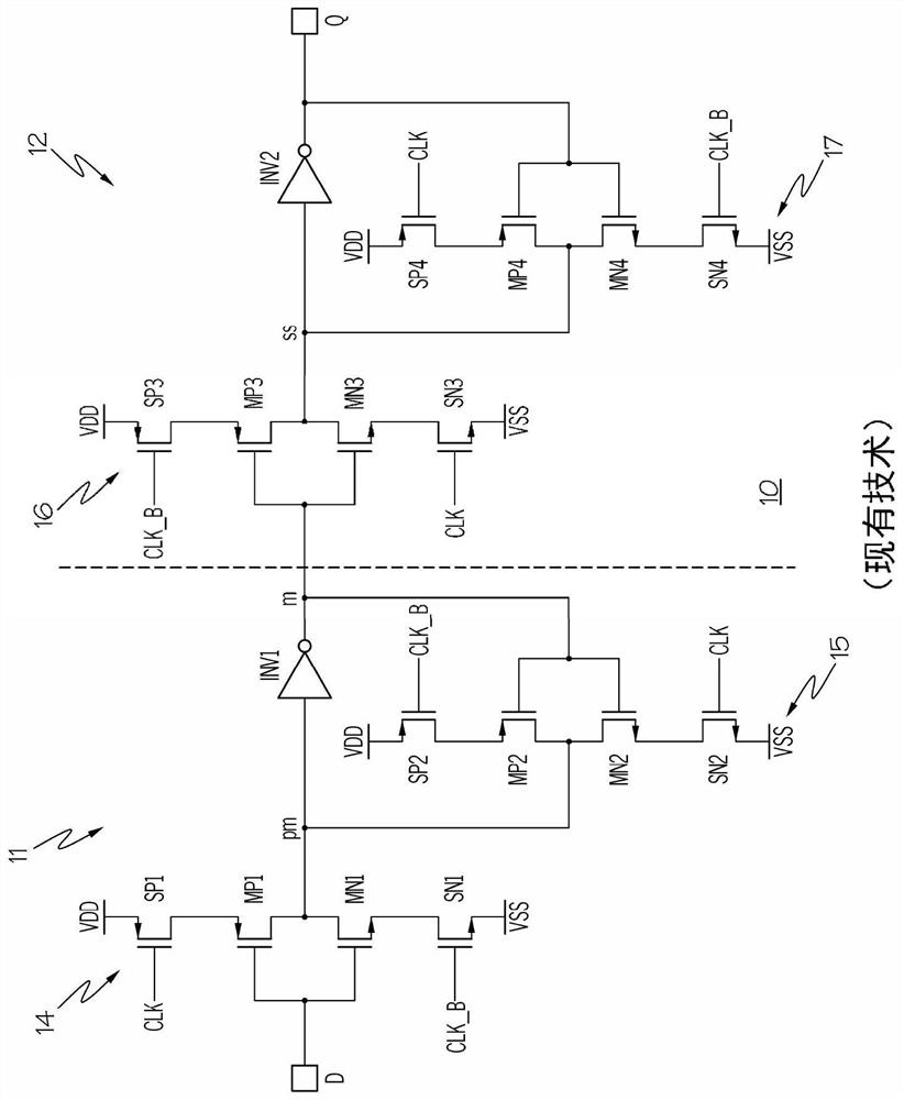
[0017] Referring now to the attached drawings, in particular to the figure 1 , shows a schematic diagram of a D flip-flop (DFF) circuit according to the prior art. As shown, the DFF circuit 10 includes a master latch 11 and a slave latch 12 . Master latch 11 includes first and second clocked inverter stages 14-15 and a first (unclocked) inverter INV1. The first clock inverter stage 14 comprises a p-channel clock switch SP1 , a p-channel data device MP1 , an n-channel data device MN1 , and an n-channel clock switch SN1 all connected in series. The second clock inverter stage 15 comprises a p-channel clock switch SP2, a p-channel data device MP2, an n-channel data device MN2, and an n-channel clock switch SN2 all connected in series. Similarly, slave latch 12 includes third and fourth clock inverter stages 16-17, clock switches SP3, SN3, SP4, and SN4 of similar configuration, and data devices MP3, MN3, MP4, and MN4, and a second (non-clocked) inverter INV2.
[0018] The in-p...
PUM
 Abstract
Description
Claims
Application Information
 - R&D Engineer
- R&D Manager
- IP Professional
- Industry Leading Data Capabilities
- Powerful AI technology
- Patent DNA Extraction
Browse by: Latest US Patents, China's latest patents, Technical Efficacy Thesaurus, Application Domain, Technology Topic, Popular Technical Reports.
© 2024 PatSnap. All rights reserved.Legal|Privacy policy|Modern Slavery Act Transparency Statement|Sitemap|About US| Contact US: help@patsnap.com


