Positioning method and positioning device for target position of semiconductor chip sample
A technology of target position and positioning method
- Summary
- Abstract
- Description
- Claims
- Application Information
AI Technical Summary
Problems solved by technology
Method used
Image

Examples
Embodiment Construction
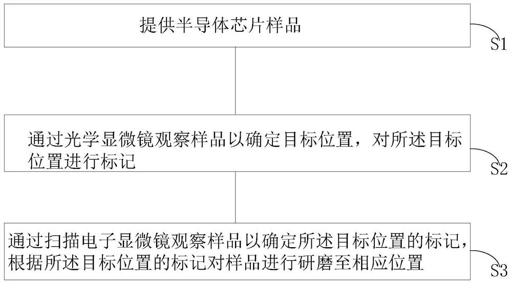
[0027] A method for locating a target position of a semiconductor chip sample and a device 1000 for locating a target position of a semiconductor chip sample proposed by the present invention will be further described in detail below with reference to the accompanying drawings and specific embodiments.
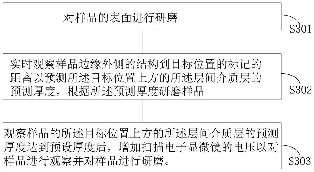
[0028] The method for locating the target position of a semiconductor chip sample according to an embodiment of the present invention will be described below with reference to the accompanying drawings. figure 1 and Figure 3-Figure 5 As shown, the positioning method of the semiconductor chip sample target position according to the embodiment of the present invention includes the following steps:
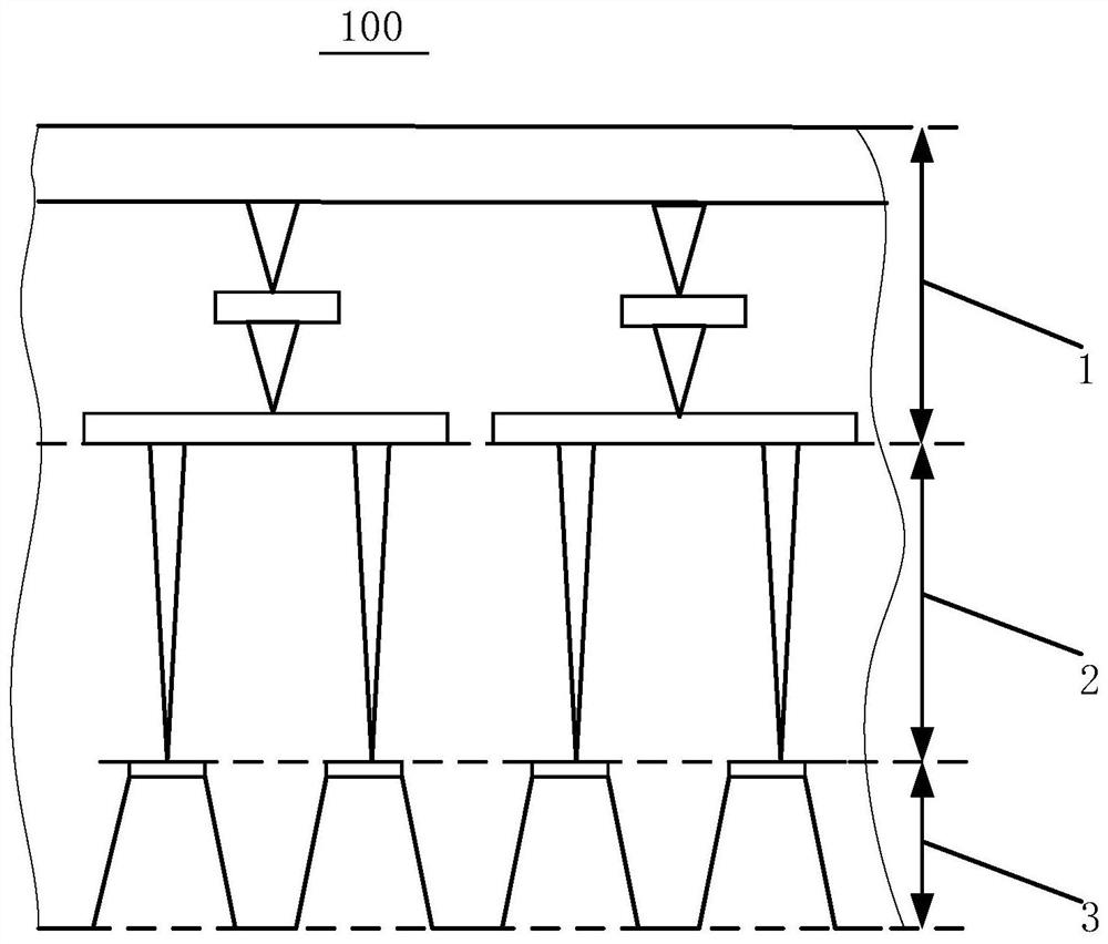
[0029] S1: provide a semiconductor chip sample 100; for the semiconductor chip sample 100, if image 3 As shown, the semiconductor chip sample 100 may include an interlayer dielectric layer 2 and a device region layer 3, the interlayer dielectric layer 2 is located above the device...
PUM
 Abstract
Description
Claims
Application Information
 - R&D Engineer
- R&D Manager
- IP Professional
- Industry Leading Data Capabilities
- Powerful AI technology
- Patent DNA Extraction
Browse by: Latest US Patents, China's latest patents, Technical Efficacy Thesaurus, Application Domain, Technology Topic.
© 2024 PatSnap. All rights reserved.Legal|Privacy policy|Modern Slavery Act Transparency Statement|Sitemap