Thin film transistor (TFT) array substrate and display device

A technology for array substrates and pixel electrode layers, applied in optics, instruments, electrical components, etc., can solve problems such as lower aperture ratio, affect transmittance and response speed, reduce transmittance, etc., to reduce cost and energy consumption, Effect of reducing liquid crystal alignment disorder area, high aperture ratio and transmittance

Inactive Publication Date: 2012-08-08
BOE TECH GRP CO LTD +1
View PDF6 Cites 44 Cited by
  • Summary
  • Abstract
  • Description
  • Claims
  • Application Information

AI Technical Summary

Problems solved by technology

The appearance of black streaks affects the transmittance and response speed
In order to improve the display effect, a wider black matrix is ​​generally made on the opposite color filter substrate to block the disordered area, which results in a decrease in the aperture ratio, thus reducing the transmittance

Method used


Image

  • Thin film transistor (TFT) array substrate and display device
  • Thin film transistor (TFT) array substrate and display device
  • Thin film transistor (TFT) array substrate and display device

Examples


Embodiment 1

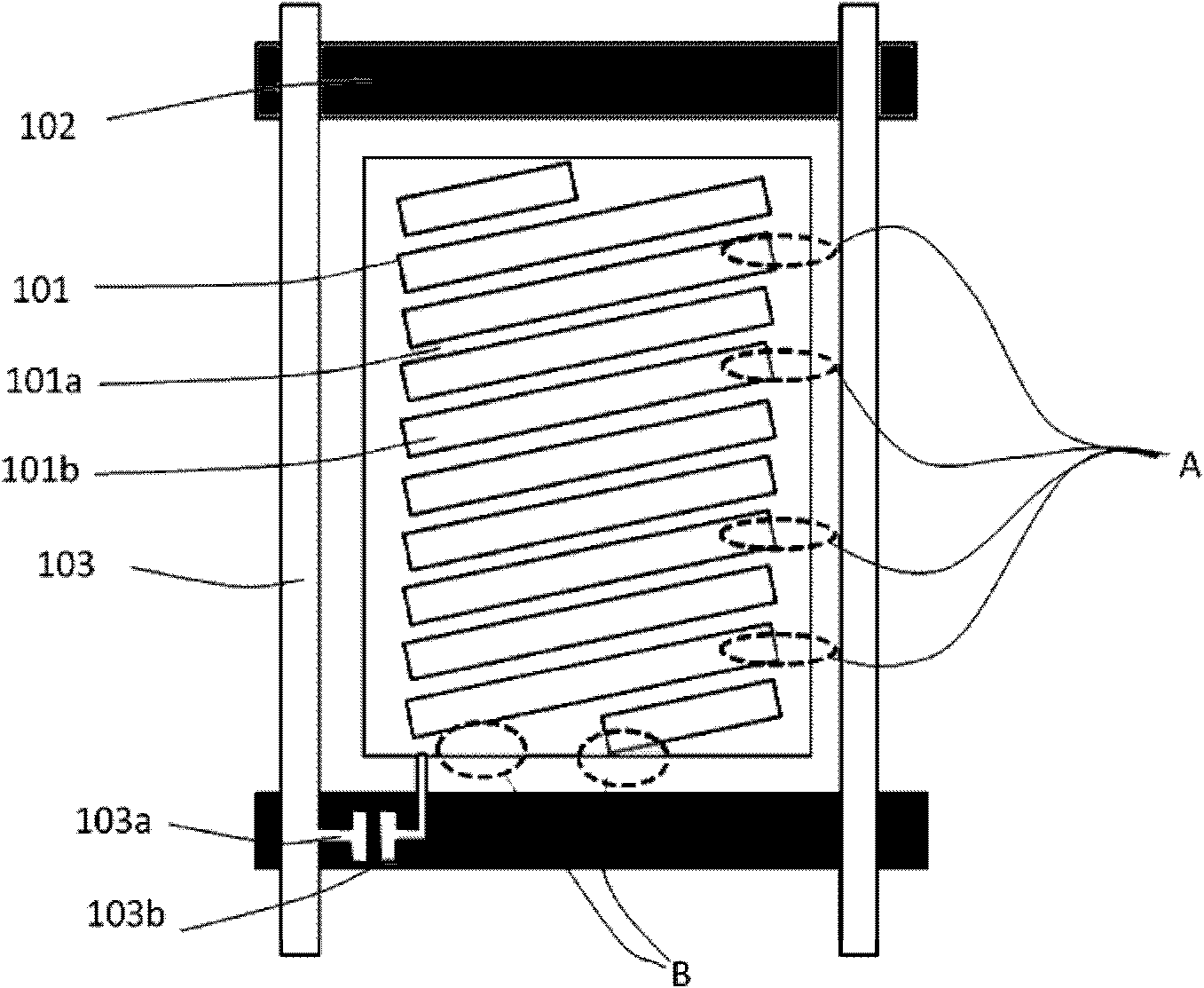
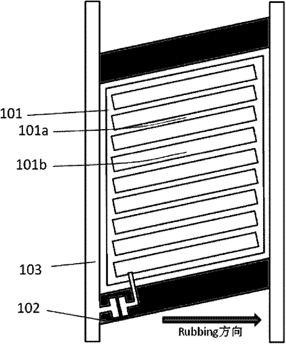
[0036] Such as image 3 As shown, it is a schematic diagram of a single sub-pixel structure in a TFT array substrate structure of the present invention, including: gate lines 102 and data lines 103 formed on the substrate (not shown in the figure); gate lines 102 and data lines 103 intersect Several sub-pixel units are defined, and each sub-pixel unit includes a thin film transistor device, a common electrode, a first pixel electrode layer and a second pixel electrode layer 101 . The second pixel electrode layer 101 has striped pixel electrodes 101 a and openings 101 b of the second pixel electrode layer 101 . One of the first pixel electrode layer and the second pixel electrode layer 101 is connected to the common electrode, and the other pixel electrode layer is connected to the source or drain of the thin film transistor, and the first pixel electrode layer and the second pixel electrode layer 101 are connected through an insulating Layers are separated. The second pixel ...

Embodiment 2

[0040] Such as Figure 5 As shown, the difference from Embodiment 1 is that the initial orientation of the liquid crystal is vertical, the data lines 103 are parallel to the striped pixel electrodes 101a, the direction of the gate lines 102 is perpendicular to the orientation of the liquid crystals, and the entire second pixel electrode layer 101 is in the shape of a parallelogram.

[0041] Such a design makes the direction of the disturbance electric field generated by the data line 103 consistent with the direction of the fringe field driving the liquid crystal in the pixel, and at the same time, the edge of the pixel electrode close to the data line 103 is parallel to the strip-shaped pixel electrode 101a inside, so that there will be no disordered electric field at the edge of the pixel The phenomenon of liquid crystal alignment disorder due to the influence of the influence of the influence, and no black streaks are generated near the data line 103, the width of the black ...

Embodiment 3

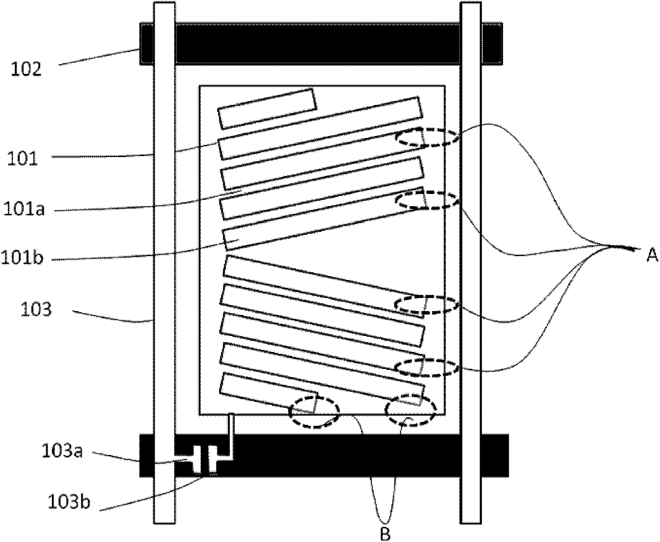
[0044] Such as Figure 7 As shown, the difference from Embodiment 1 is that the strip-shaped pixel electrodes 101a on the second pixel electrode layer 101 are divided into two symmetrical groups, and the respective strip-shaped pixel electrodes 101a in each group are parallel. The gate line 102 is parallel to a group of strip-shaped pixel electrodes 101a close to it in the second pixel electrode layer, and the entire second pixel electrode layer 101 is trapezoidal.

[0045] Such a design makes the direction of the disturbing electric field generated by the gate line 102 consistent with the direction of the fringe field driving the liquid crystal in the pixel, and at the same time, the edge of the pixel electrode near the gate line 102 is parallel to the strip-shaped pixel electrode 101a inside, so that there will be no disordered electric field at the edge of the pixel. The liquid crystal alignment disorder phenomenon is caused by the influence of the influence, and no black s...


PUM

PropertyMeasurementUnit
angleaaaaaaaaaa
angleaaaaaaaaaa

Abstract

The invention discloses a thin film transistor (TFT) array substrate, which comprises grid lines and data lines, the grid lines and the data lines are formed on the substrate. The grid lines and the data lines cross to define sub-pixel units. Each sub-pixel unit comprises a thin film transistor device, a public electrode, a first pixel electrode layer and a second pixel electrode layer. The first pixel electrode layers or the second pixel electrode layers are connected with public electrodes, and the other ones are connected with source electrodes or drain electrodes of the thin film transistors, the first pixel electrode layers and the second pixel electrode layers are separated through insulation layers, and the second pixel electrode layers are arranged above the first pixel electrode layers. Images of strip pixel electrodes of the second pixel electrode layers are overlapped with images of the first pixel electrode layers, an inclined angle is arranged between the strip pixel electrodes and liquid crystal initial orientation, and the grid lines are parallel to the strip pixel electrodes close to the grid lines or the data lines are parallel to the strip pixel electrodes close to the data lines. The TFT array substrate and the display device guarantee that a liquid crystal orientation chaos phenomenon caused by effects of disorder electric fields at a pixel edge can not occur.

Description

technical field [0001] The invention relates to the technical field of thin film transistor liquid crystal display, in particular to a TFT array substrate and a display device. Background technique [0002] TN, IPS, VA, and ADS are several modes of liquid crystal display. Among them, ADS is the abbreviation of ADSDS (ADvanced Super Dimension Switch), that is, advanced super-dimensional field switching technology, through the electric field generated by the edge of the slit electrode in the same plane and The electric field generated between the slit electrode layer and the plate electrode layer forms a multi-dimensional electric field, so that all oriented liquid crystal molecules between the slit electrodes in the liquid crystal cell and directly above the electrodes can be rotated, thereby improving the working efficiency of the liquid crystal and increasing the light transmission efficiency. Advanced ultra-dimensional field switching technology can improve the picture qu...

Claims


Application Information

Patent Timeline
Patent Type & Authority Applications(China)
IPC IPC(8): G02F1/1362G02F1/1368G02F1/1343G02F1/139H01L27/02
CPCG02F1/1343G02F1/134363G02F1/136286G02F1/134372
Inventor 孙荣阁
Owner BOE TECH GRP CO LTD
Why Eureka
Try Eureka