IPM packaging method and bonding method in IPM packaging

A bonding and bonding process technology, applied in the field of bonding, can solve problems such as low yield, improve yield and performance, avoid poor insulation performance, and avoid poor voltage resistance.

Pending Publication Date: 2020-10-27
WUXI CHINA RESOURCE MICRO ASSEMBLY TECH
View PDF11 Cites 0 Cited by
  • Summary
  • Abstract
  • Description
  • Claims
  • Application Information

AI Technical Summary

Problems solved by technology

[0003] However, when the existing IPM packaging structure is inspected for yield, the problem of low yield often occurs

Method used


Image

  • IPM packaging method and bonding method in IPM packaging
  • IPM packaging method and bonding method in IPM packaging
  • IPM packaging method and bonding method in IPM packaging

Examples


Embodiment Construction

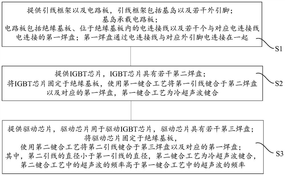
[0043] The inventor researched and analyzed the IPM packaging process, and found that one of the reasons for the low IPM yield rate is that the driver chip requires more and thinner leads, so gold wires, copper wires, etc. are generally used between the driver chip and the circuit board for thermal ultrasonic wire bonding; thermal ultrasonic bonding requires high temperature heating in the equipment track, high temperature will cause the insulating substrate carrying the IGBT chip to separate from the base island, tearing, on the one hand, the tearing of the insulating substrate will cause the bottom of the IGBT chip The breakdown between the electrode and the base island results in poor breakdown resistance of the IPM, that is, poor voltage resistance; on the other hand, the IGBT chip is separated from the base island, which affects the heat dissipation performance.

[0044] In order to make the above objects, features and advantages of the present invention more comprehensibl...


PUM

PropertyMeasurementUnit
Diameteraaaaaaaaaa
Diameteraaaaaaaaaa

Abstract

The invention provides an IPM packaging method and a bonding method in IPM packaging, wherein first cold ultrasonic bonding is carried out on a first lead wire with a relatively large diameter betweenan IGBT chip and a circuit board by adopting ultrasonic waves with a relatively low frequency, and second cold ultrasonic bonding is carried out on a second lead wire with a relatively small diameterbetween a driving chip and the circuit board by adopting ultrasonic waves with a relatively high frequency. According to the invention, cold ultrasonic bonding is adopted without heating compared with thermal ultrasonic bonding of a gold-copper wire, so that the separation of an insulating substrate for bearing an IGBT chip and a driving chip from a base island caused by high-temperature heatingcan be avoided, the worsening of the insulating performance caused by tearing of the insulating substrate in the separation process can be avoided, the problems of poor IPM voltage resistance, poor heat dissipation and the like can be avoided, and the IPM yield and performance can be improved.

Description

technical field [0001] The invention relates to the technical field of chip packaging, in particular to an IPM packaging method and a bonding method in the IPM packaging. Background technique [0002] Intelligent Power Module (IPM) is a new type of control module that integrates an Insulated Gate Bipolar Transistor (IGBT) chip and its drive circuit. It has the advantages of low cost, miniaturization, high reliability, and easy use, and is widely used in frequency conversion home appliances, inverter power supplies, industrial control and other fields. [0003] However, the existing IPM package structure often suffers from a low yield rate during yield inspection. [0004] In view of this, the present invention provides a new IPM packaging method and a bonding method in the IPM packaging, so as to improve the yield rate of the IPM. Contents of the invention [0005] The purpose of the present invention is to provide an IPM packaging method and a bonding method in the IPM ...

Claims


Application Information

Patent Timeline
IPC IPC(8): H01L25/16H01L23/495H01L21/607
CPCH01L25/16H01L25/50H01L23/4952H01L23/49575H01L24/85H01L2224/85205H01L2224/85181H01L2224/48472H01L2224/78313H01L2224/48091H01L2924/00014
Inventor 王永庭
Owner WUXI CHINA RESOURCE MICRO ASSEMBLY TECH
Why Eureka
Try Eureka