Data scheduling method and device for PCIE switching chip port

A switching chip, data scheduling technology, applied in the direction of electrical digital data processing, instruments, etc., can solve the problem of less disclosure of information in the application layer implementation mechanism of PCIE switching chip

Active Publication Date: 2020-10-30
牛芯半导体(深圳)有限公司
View PDF2 Cites 3 Cited by
  • Summary
  • Abstract
  • Description
  • Claims
  • Application Information

AI Technical Summary

Problems solved by technology

[0004] Although there are many PCIE switch chips on the market, there are very few disclosures on the application layer implementation mechanism of PCIE switch chips

Method used


Image

  • Data scheduling method and device for PCIE switching chip port
  • Data scheduling method and device for PCIE switching chip port
  • Data scheduling method and device for PCIE switching chip port

Examples


Embodiment Construction

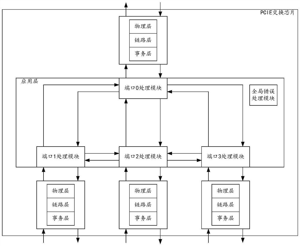
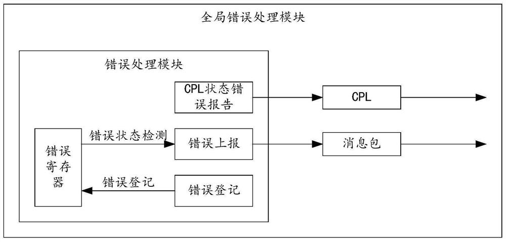
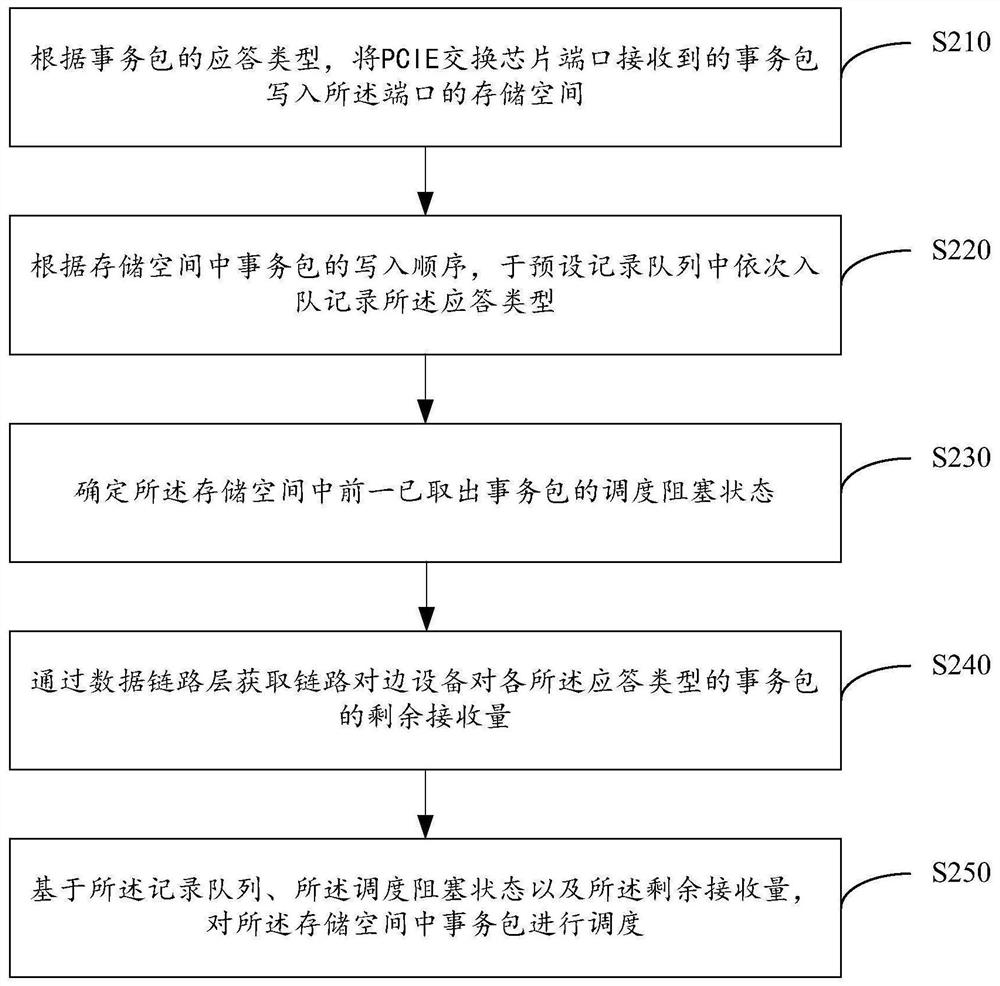
[0030] Example embodiments will now be described more fully with reference to the accompanying drawings. Example embodiments may, however, be embodied in many forms and should not be construed as limited to the examples set forth herein; Fully conveyed to those skilled in the art. The drawings are merely schematic illustrations of the present disclosure and are not necessarily drawn to scale. The same reference numerals in the drawings denote the same or similar parts, and thus repeated descriptions thereof will be omitted.

[0031] Furthermore, the described features, structures, or characteristics may be combined in any suitable manner in one or more example embodiments. In the following description, numerous specific details are provided in order to give a thorough understanding of example embodiments of the present disclosure. However, those skilled in the art will appreciate that the technical solutions of the present disclosure may be practiced without one or more of ...


PUM


Abstract

The invention provides a data scheduling method and device for a PCIE switching chip port, and the method comprises the steps of writing a transaction package received by the PCIE switching chip portinto a storage space of the port according to the response type of the transaction package; sequentially enqueueing and recording the response types in a preset recording queue according to the writing sequence of the transaction packages in the storage space; determining a scheduling blocking state of a previous extracted transaction packet in the storage space; obtaining the residual receiving quantity of the link opposite side equipment for the transaction packets of the response types through a data link layer; and based on the record queue, the scheduling blocking state and the residual receiving amount, scheduling the transaction packet in the storage space. According to the embodiment of the invention, the accuracy of data scheduling of the PCIE switching chip port can be ensured.

Description

technical field [0001] The present disclosure relates to the chip field, in particular to a data scheduling method and device for a port of a PCIE switch chip. Background technique [0002] PCIE (PCI-Express, peripheral component interconnect express) is a high-speed serial computer expansion bus standard. It is the third-generation I / O bus after the PCI bus. It is widely used in communication devices such as CPUs, graphics cards, and sound cards. [0003] Among them, the response types of the transaction packets of the PCIE chip port are divided into three types: P (Posted, forwarding), NP (Non-Posted, non-posted) and CPL (Completion, completion). Wherein, after the request of the NP transaction packet is sent out, the response of a CPL transaction packet must be obtained before the transmission ends; after the request of the P transaction packet is sent out, the response of the CPL transaction packet does not need to be obtained. The forwarding order of these three types ...

Claims


Application Information

Patent Timeline
IPC IPC(8): G06F13/16G06F13/42
CPCG06F13/1642G06F13/4282G06F2213/0026
Inventor 崔飞飞张建波赵姣杨珂
Owner 牛芯半导体(深圳)有限公司
Why Eureka
Try Eureka