
Schottky diode and preparation method thereof

A Schottky diode and Schottky contact technology, applied in the field of diodes, can solve the problems of dissipating input power, increasing resistance, affecting frequency doubling efficiency, etc., so as to improve reverse bias breakdown voltage and increase power withstand capacity. Effect

Active Publication Date: 2020-10-30
NUCTECH CO LTD
View PDF4 Cites 1 Cited by
  • Summary
  • Abstract
  • Description
  • Claims
  • Application Information

AI Technical Summary

Problems solved by technology

For traditional Schottky diodes, the current has a strong congestion effect when passing through the Schottky junction, causing the resistance to increase, dissipating the input power, reducing the power capacity of the Schottky diode, and thus affecting its frequency doubling efficiency

Method used

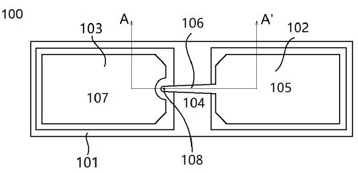
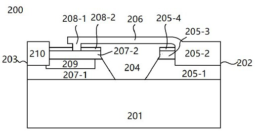
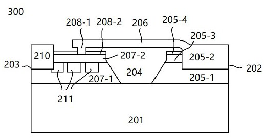

Image

  • Schottky diode and preparation method thereof
  • Schottky diode and preparation method thereof
  • Schottky diode and preparation method thereof

Examples


Embodiment Construction

[0019] The following detailed description of the embodiments of the present disclosure covers numerous specific details in order to provide a thorough understanding of the present invention. It will be apparent, however, to one skilled in the art that embodiments of the present disclosure may be practiced without some of these specific details. The following description of the embodiments is only to provide a clearer understanding of the present invention by showing examples of the present invention. The present invention is in no way limited to any specific configuration and method steps set forth below, but covers any modification, substitution and improvement of related elements, components and method steps without departing from the teaching of the present invention.

[0020] The power capacity output of the frequency doubler can be improved by increasing the number of Schottky diodes or increasing the area of ​​the Schottky junction. However, increasing the number of Scho...


PUM

PropertyMeasurementUnit
thicknessaaaaaaaaaa
thicknessaaaaaaaaaa
thicknessaaaaaaaaaa

Abstract

The invention relates to a Schottky diode and a preparation method thereof. A Schottky diode includes: a substrate layer; a first structure and a second structure which are located on the substrate layer, wherein an isolation groove structure is arranged between the first structure and the second structure, the first structure comprises a first main body region and a cantilever beam extending fromthe first main body region, the second structure comprises a second main body region, and the second main body region comprises a heavily doped layer located on the substrate layer and a lightly doped layer located on the heavily doped layer; and a Schottky contact structure including a contact metal layer on the lightly doped layer and connected to an end portion of the cantilever beam and a passivation layer on the lightly doped layer and surrounding the contact metal layer, wherein the heavily doped layer has one or more regions in a position corresponding to the contact metal layer, the one or more regions being in contact with the lightly doped layer and forming depletion regions at the contact interface with corresponding regions of the lightly doped layer.

Description

technical field [0001] The invention relates to the technical field of diodes, in particular to a Schottky diode and a preparation method thereof. Background technique [0002] Terahertz waves refer to electromagnetic waves with a frequency in the range of 100GHz-l0THz, which overlap with the high-end of millimeter waves, submillimeter waves and far infrared, and are in the transitional field from macroelectronics to microphotonics. In the low-end range of terahertz frequencies, the solid-state source is usually obtained by multiplying millimeter waves to the terahertz frequency band through nonlinear semiconductor devices. [0003] There are many advantages to using Schottky diode devices to achieve high-efficiency frequency multiplication. At the same time, Schottky diode devices can work stably in the entire millimeter wave and submillimeter wave frequency bands from 30GHz to 3000GHz. Therefore, Schottky diode high-efficiency frequency multiplication technology is very su...

Claims


Application Information

Patent Timeline
Patent Type & Authority Applications(China)
IPC IPC(8): H01L29/872H01L21/329H01L29/06
CPCH01L29/0615H01L29/0684H01L29/66212H01L29/872
Inventor 赵自然胡海帆马旭明肖雄
Owner NUCTECH CO LTD
Learn More