
Buffer-free optical interconnect architecture and method for data center

A buffer-free, optical interconnect technology, applied in multiplexing communications, wavelength division multiplexing systems, optical multiplexing systems, etc., and can solve problems such as high power consumption and multiple device configuration times.

Active Publication Date: 2020-10-30
ZHEJIANG UNIV +1
View PDF3 Cites 3 Cited by
  • Summary
  • Abstract
  • Description
  • Claims
  • Application Information

AI Technical Summary

Problems solved by technology

It solves the technical problems of many traditional data center network devices, long configuration time, and high power consumption, and achieves the goal of low latency and high reliability under the premise of high throughput

Method used


Image

  • Buffer-free optical interconnect architecture and method for data center
  • Buffer-free optical interconnect architecture and method for data center
  • Buffer-free optical interconnect architecture and method for data center

Examples


Embodiment Construction

[0059] The present invention will be further described below in conjunction with drawings and embodiments.

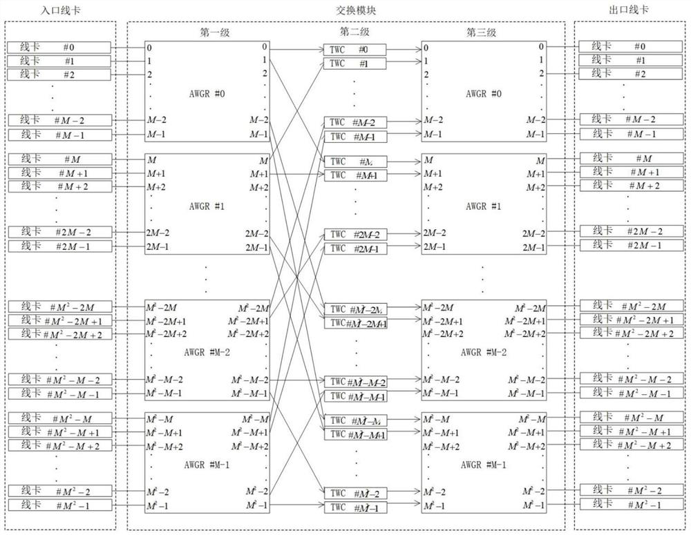
[0060] Such as figure 1 As shown, the architecture of the present invention is divided into an entrance line card, a three-level switch module and an exit line card. The switch module is composed of a first-level AWGR, a second-level TWC, and a third-level AWGR; M first-level AWGRs and M first-level AWGRs Each of the three-level AWGR has M input ports and output ports, each input port of the first-level AWGR is connected to an inlet line card, and each output port of the third-level AWGR is connected to an outlet line card, An output port of the first-stage AWGR and an input port of the third-stage AWGR are connected through a second-stage TWC.

[0061] The number of single-ended ports of an AWGR device is M, and the ingress line card and the egress line card are respectively M 2 , respectively for them from 0 to M 2 -1 for number sorting; there are M first-level and...


PUM


Abstract

The invention discloses a buffer-free optical interconnection architecture and method for a data center. The architecture is divided into an inlet wire clamp, a three-stage exchange module and an outlet wire clamp, wherein the exchange module comprises a first-stage AWGR, a third-stage AWGR and a second-stage TWC; the first-stage AWGR input port is provided with an inlet wire clamp, the third-stage AWGR output port is provided with an outlet wire clamp, and the first-stage AWGR output port and the third-stage AWGR input port are connected through a second-stage TWC. Signals of the server are subjected to wavelength division multiplexing and then forwarded to the switching module through wavelength modulation of the entrance line card, optical signals with specific wavelengths are forwardedto the exit line card through TWC wavelength conversion and AWGR cyclic routing, and the exit line card processes the optical signals and then sends the optical signals to the server. High-capacity,high-reliability and low-power-consumption all-optical interconnection is achieved, a data center is effectively flattened, the defects that a traditional space switch is low in port bandwidth and limited in port number are overcome, and the all-optical interconnection system has the advantages of being high in reliability, low in complexity, low in delay and the like.

Description

technical field [0001] The invention belongs to an optical interconnection structure and an optical communication method of an optical switching network in a data center, and relates to a bufferless optical backplane realization method for optical switching in a wavelength domain. Background technique [0002] Optical backplanes have been widely used in data center optical networks. In the past decade, many improvements have been applied to the data center optical backplane architecture in order to cope with the rapid growth of interconnected nodes and traffic. Including the use of passive orthogonal electrical intermediate boards to connect line cards and switch cards to build a three-level non-blocking Clos network; use concentrically arranged optical buses to form optical fiber rings to interconnect more nodes. However, due to the technical limitations of devices, the bandwidth and the number of interconnected nodes achieved by these methods are limited. In order to redu...

Claims


Application Information

Patent Timeline
IPC IPC(8): H04J14/02
CPCH04J14/0267H04J14/0272H04J14/022H04J14/0254
Inventor 杨晓雪胡冰
Owner ZHEJIANG UNIV
Learn More