
Waste discharge device capable of avoiding damage to circuit unit for printed circuit board processing

A technology of a waste discharge device and a circuit unit, which is applied to cleaning methods and appliances, cleaning methods using tools, and cleaning methods using gas flow, etc., which can solve problems such as low cleaning efficiency, inability to clean waste, and insufficient cleaning. Achieve fast and efficient cleaning, improve waste discharge efficiency, and high cleaning efficiency

Inactive Publication Date: 2020-11-10
王钟
View PDF11 Cites 0 Cited by
  • Summary
  • Abstract
  • Description
  • Claims
  • Application Information

AI Technical Summary

Problems solved by technology

[0007] The purpose of the present invention is to provide a waste discharge device for circuit board processing that can avoid damage to circuit units, so as to solve the problem that most of the circuit board waste discharge devices proposed in the above background technology tend to cause damage to circuit unit devices during waste discharge. And it is impossible to clean up the waste sticking on the surface of the circuit board, so that the cleaning is not clean enough, and the cleaning efficiency is low, and the problem of fast and efficient cleaning cannot be achieved

Method used


Image

  • Waste discharge device capable of avoiding damage to circuit unit for printed circuit board processing
  • Waste discharge device capable of avoiding damage to circuit unit for printed circuit board processing
  • Waste discharge device capable of avoiding damage to circuit unit for printed circuit board processing

Examples


Embodiment Construction

[0034] The technical solutions in the embodiments of the present invention will be clearly and completely described below in conjunction with the accompanying drawings in the embodiments of the present invention. Obviously, the described embodiments are only some of the embodiments of the present invention, not all of them. Based on The embodiments of the present invention and all other embodiments obtained by persons of ordinary skill in the art without making creative efforts belong to the protection scope of the present invention.

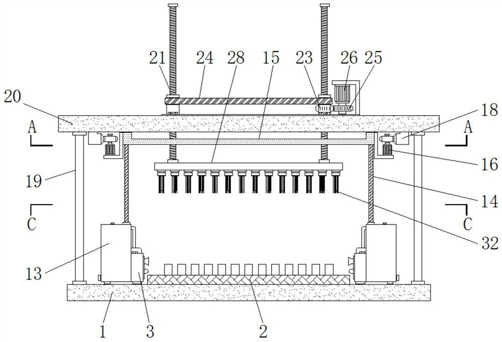
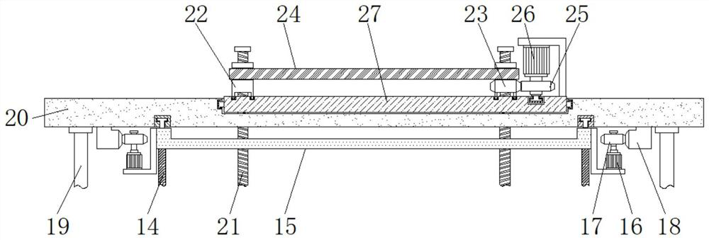
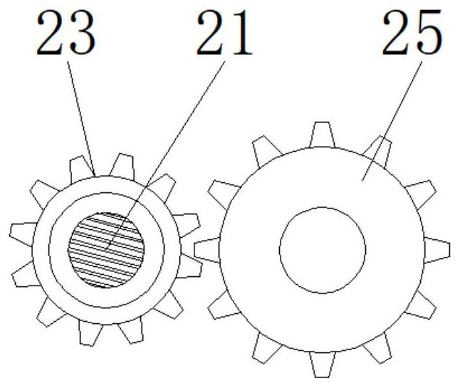
[0035] see Figure 1-9 , the present invention provides a technical solution: a circuit board processing waste discharge device capable of avoiding damage to the circuit unit, comprising a bottom plate 1, a circuit board 2, a connection box 3, a material receiving port 4, a blowing port 5, a first filter plate 6. The first buffer box 7, the second buffer box 8, the first connecting pipe 9, the second connecting pipe 10, the second filter plate 1...


PUM


Abstract

The invention discloses a waste discharge device capable of avoiding damage to a circuit unit for printed circuit board processing. The waste discharge device comprises a bottom plate, suction and blowing fans, a top plate and a bearing plate, wherein a printed circuit board is arranged on the bottom plate, and connecting boxes are arranged on the left side and the right side of the printed circuit board; material absorption openings are formed in the inner side surfaces of the connecting boxes, the outer sides of the material absorption openings are connected with first buffer boxes, and theupper ends of the first buffer boxes are connected with first connecting pipes; and the upper ends of second buffer boxes are provided with the tail ends of second connecting pipes, and second filterplates are arranged inside the upper ends of the second connecting pipes. According to the waste discharge device capable of avoiding damage to the circuit unit for printed circuit board processing, damage to circuit unit components can be avoided during waste discharge, and waste chips adhering to the surface of the printed circuit board can be removed, so that cleaning is thorough enough, the cleaning efficiency is high, and rapid and efficient cleaning can be achieved.

Description

technical field [0001] The invention relates to the technical field related to circuit board processing, in particular to a waste discharge device for circuit board processing that can avoid damage to circuit units. Background technique [0002] The circuit board is an essential structure in electrical appliances. When the circuit board is processed, a certain amount of waste is often generated. If the waste is not disposed of in time, it will affect the subsequent processing and some functions of the circuit board. Therefore, A waste discharge device is needed to clean up the waste generated during circuit board processing, but the existing circuit board waste discharge device still has certain defects, such as: [0003] 1. The surface of the circuit board usually has more circuit unit devices during processing, and the general circuit board waste discharge device often easily causes damage to the circuit unit devices during waste discharge; [0004] 2. The existing circui...

Claims


Application Information

Patent Timeline
IPC IPC(8): B08B5/02B08B1/00B08B15/04
CPCB08B5/02B08B15/04B08B1/30
Inventor 王钟
Owner 王钟
Learn More