
Organic el device and production method therefor

A manufacturing method, an organic technology, applied in the direction of identification device, lighting device, semiconductor/solid-state device manufacturing, etc., can solve the problem of low mass production, and achieve the effect of improving the reliability of moisture resistance

Active Publication Date: 2020-11-13
SAKAI DISPLAY PROD
View PDF23 Cites 0 Cited by
  • Summary
  • Abstract
  • Description
  • Claims
  • Application Information

AI Technical Summary

Problems solved by technology

Since the formation of the organic barrier layer using printing technology is carried out in the atmosphere or nitrogen atmosphere, the formation of the inorganic barrier layer is carried out in a vacuum. Therefore, in the process of forming the thin film sealing structure, the element substrate is taken out from the vacuum chamber and placed in the vacuum chamber. , so the mass production is low

Method used


Image

  • Organic el device and production method therefor
  • Organic el device and production method therefor
  • Organic el device and production method therefor

Examples


Embodiment Construction

[0047] Hereinafter, an organic EL display device and a manufacturing method thereof according to an embodiment of the present invention will be described with reference to the drawings. Hereinafter, an OLED display device having a flexible substrate is exemplified, but embodiments of the present invention are not limited to organic EL display devices, and other organic EL devices such as organic EL lighting devices may also be used, and are not limited to the following exemplified embodiments.

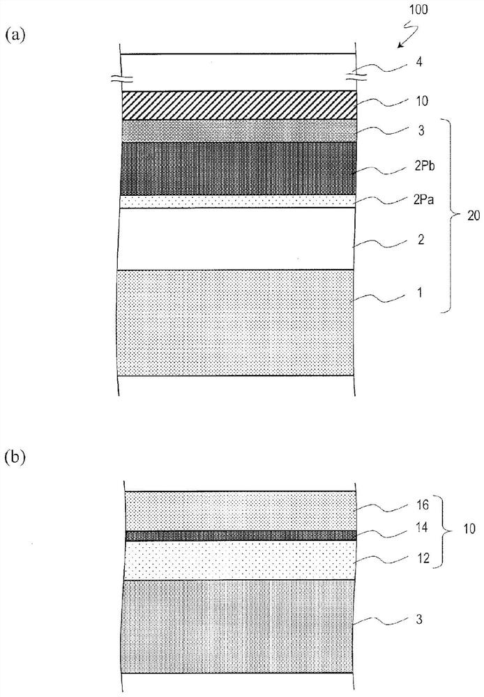
[0048] First, refer to figure 1 (a) and (b) illustrate the basic configuration of the OLED display device 100 according to the embodiment of the present invention. figure 1 (a) is a schematic partial cross-sectional view of an active region of an OLED display device 100 according to an embodiment of the present invention, figure 1 (b) is a partial cross-sectional view of the TFE structure 10 formed on the OLED3.

[0049] The OLED display device 100 has a plurality of pixels, and each...


PUM

PropertyMeasurementUnit
surface roughnessaaaaaaaaaa
thicknessaaaaaaaaaa

Abstract

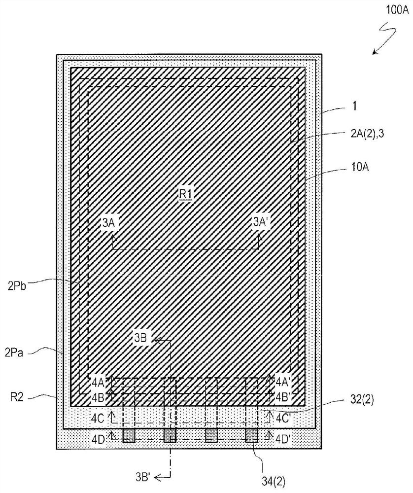
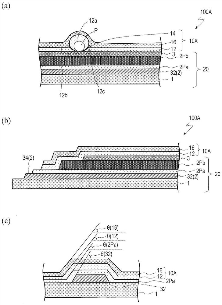
This organic EL device (100) has a substrate (1), a drive circuit layer (2), a first inorganic protective layer (2Pa), an organic planarizing layer (2Pb), an organic EL element layer (3), a second inorganic protective layer (2Pa2), and a TFE structure (10). The TFE structure has a first inorganic barrier layer (12), an organic barrier layer (14), and a second inorganic barrier layer (16). When viewed from a normal line of the substrate, the organic planarizing layer is formed within a region where the first inorganic protective layer is formed, while an organic EL element is disposed within aregion where the organic planarizing layer is formed. The TFE structure has an exterior edge which intersects with a lead-out line (32) and which is situated between an exterior edge of the organic planarizing layer and an exterior edge of the first inorganic protective layer. In a portion where the first inorganic protective layer and the first inorganic barrier layer are in direct contact with each other on the lead-out line, the first inorganic barrier layer has, in a cross-section parallel to the line width direction of the lead-out line, a lateral face that is configured to have a taper angle theta (12) of less than 90 DEG. The organic planarizing layer has a surface which exceeds 50 nm in arithmetic average roughness Ra, while the second inorganic protective layer has a surface thatis not more than 50 nm in arithmetic average roughness Ra.

Description

technical field [0001] The present invention relates to an organic EL device (for example, an organic EL display device and an organic EL lighting device) and a manufacturing method thereof. Background technique [0002] Organic EL (ElectroLuminescence, electroluminescence) display devices have begun to be put into practical use. One characteristic of the organic EL display device is that a flexible display device can be obtained. The organic EL display device has at least one organic EL element (Organic Light Emitting Diode: OLED, Organic Light Emitting Diode) for each pixel and at least one TFT (Thin Film Transistor, thin film transistor) that controls the current supplied to each OLED. Hereinafter, the organic EL display device is referred to as an OLED display device. As described above, for each OLED, an OLED display device having a switching element such as a TFT is called an active matrix type OLED display device. In addition, the substrates on which TFTs and OLEDs...

Claims


Application Information

Patent Timeline
Patent Type & Authority Applications(China)
IPC IPC(8): H05B33/04G09F9/30H01L27/32H01L51/50H05B33/02H05B33/06H05B33/22
CPCH10K59/873H10K59/8731H01L27/124H01L27/1259H10K59/124H10K59/123H10K59/131H10K59/1201H10K71/00G09F9/335G09F9/301G09F9/30H05B33/02H05B33/04H05B33/06H05B33/22H10K50/844H10K59/1213
Inventor 岸本克彦鸣泷阳三
Owner SAKAI DISPLAY PROD
Learn More