Organic el device and production method therefor

An EL device and organic technology, applied in the field of organic EL devices and their manufacturing, can solve the problem of not having a thick organic barrier layer, etc., and achieve the effect of improving moisture resistance and reliability

Inactive Publication Date: 2020-10-16
SAKAI DISPLAY PROD
View PDF22 Cites 0 Cited by
  • Summary
  • Abstract
  • Description
  • Claims
  • Application Information

AI Technical Summary

Problems solved by technology

The thin film encapsulation structure described in Patent Document 1 or 2 does not have a thick organic barrier layer

Method used


Image

  • Organic el device and production method therefor
  • Organic el device and production method therefor
  • Organic el device and production method therefor

Examples


no. 1 approach

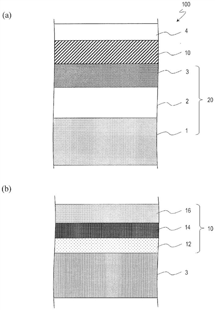
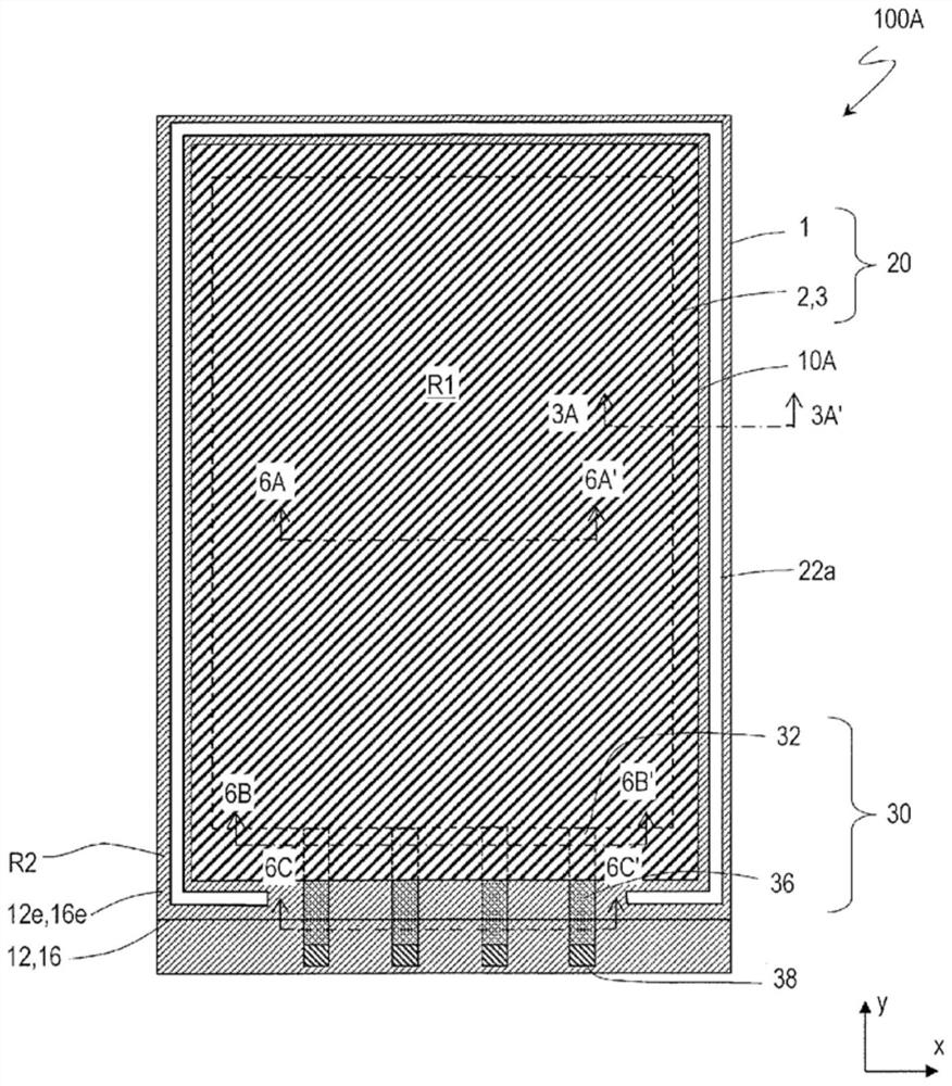
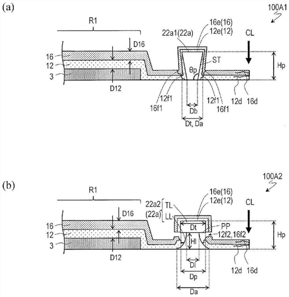
[0062] refer to Figure 2 to Figure 4 , the structure of the OLED display device 100A according to the first embodiment of the present invention and its manufacturing method will be described.

[0063] figure 2 It is a top view schematically showing an OLED display device 100A according to an embodiment of the present invention. image 3 (a) and (b) are along figure 2 Sectional view of line 3A-3A' in. image 3 (a) and (b) are cross-sectional views schematically showing OLED display devices 100A1 and 100A2 each having a protruding structure 22a1 and a protruding structure 22a2 as examples of the protruding structure 22a. The protruding structures 22a1 and 22a2 are sometimes collectively referred to as the protruding structures 22a. Sometimes the OLED display devices 100A1 and 100A2 are collectively referred to as the OLED display device 100A.

[0064] Such as figure 2 As shown, the OLED display device 100A has: a flexible substrate 1 , a circuit (backplane) 2 formed on...


PUM

PropertyMeasurementUnit
thicknessaaaaaaaaaa
thicknessaaaaaaaaaa
thicknessaaaaaaaaaa

Abstract

An organic EL device (100A) comprises a peripheral region (R2) and an active region (R1) containing a plurality of organic EL elements (3), and includes an element substrate (20) having a plurality oforganic EL elements, and a thin film seal structure (10A) covering the plurality of organic EL elements. The thin film seal structure comprises a first inorganic barrier layer (12), an organic barrier layer (14) in contact with the upper surface of the first inorganic barrier layer, and a second inorganic barrier layer (16) in contact with the upper surface of the first inorganic barrier layer and the upper surface of the organic barrier layer. The peripheral region comprises a first protruding structure (22a) containing a section extending along at least one edge of the active region, and anextending section (12e) of the first inorganic barrier layer extending over the first protruding structure. The first protruding structure includes a first part and second part. The first part is closer to the top portion of the first protruding structure than the second part and, as observed from the normal direction to the base board, a cross section parallel to the substrate surface of the first part includes a part that does not overlap with the cross section parallel to the substrate surface of the second part.

Description

technical field [0001] The invention relates to an organic EL device and a manufacturing method thereof. Background technique [0002] Organic EL (Electro Luminescence, electroluminescence) display devices have begun to be put into practical use. One of the characteristics of organic EL display devices is that flexible display devices are available. The organic EL display device has at least one organic EL element (Organic Light Emitting Diode: OLED) and at least one TFT (Thin Film Transistor, thin film transistor) for controlling the current supplied to each OLED in each pixel. Hereinafter, the organic EL display device is referred to as an OLED display device. An OLED display device having a switching element such as a TFT in each OLED as described above is called an active matrix type OLED display device. In addition, the substrate on which the TFT and OLED are formed is referred to as an element substrate. [0003] OLEDs (especially organic light-emitting layers and ...

Claims


Application Information

Patent Timeline
Patent Type & Authority Applications(China)
IPC IPC(8): H05B33/04G09F9/30H01L27/32H01L51/50H05B33/10H05B33/22
CPCG09F9/30H05B33/04H05B33/10H05B33/22H10K59/00H10K59/122H10K71/80H10K50/8445H10K71/851H10K71/861H10K50/844H10K59/121H10K59/131H10K71/00
Inventor 岸本克彦
Owner SAKAI DISPLAY PROD
Why Eureka
Try Eureka