Dedusting and deashing device for circuit board welded with components

A cleaning device and circuit board technology, applied in the direction of cleaning methods, cleaning methods and utensils, chemical instruments and methods using gas flow, etc., can solve problems such as high labor intensity, circuit board short circuit, polluted air, etc., and achieve the goal of working environment Good, comprehensive dust removal, simple structure effect

Inactive Publication Date: 2020-11-17
PUJIANG LECHENG ELECTRONICS TECH CO LTD
View PDF0 Cites 3 Cited by
  • Summary
  • Abstract
  • Description
  • Claims
  • Application Information

AI Technical Summary

Problems solved by technology

[0002] The circuit board can be called a printed circuit board or a printed circuit board, which is a circuit component that welds various circuits to a board; in addition to welding the circuit, various electronic components are also welded on the circuit board, and after welding, it may be necessary If it is placed for a long time, a lot of dust will often accumulate at this time, and the dust must be removed during use, otherwise it may cause the circuit board to be short-circuited and damaged, and the general method of dust removal is to manually hold a hair dryer against the circuit Board air blowing dust removal, this method is labor-intensive and the dust removal effect is not good, obviously it is not suitable for the dust removal operation of a large number of circuit boards, and a large amount of dust blown by the blower will still accumulate inside the warehouse, which not only pollutes the inside of the warehouse The air is also easy to accumulate on the circuit board again. The present invention illustrates a device that can solve the above problems

Method used


Image

  • Dedusting and deashing device for circuit board welded with components
  • Dedusting and deashing device for circuit board welded with components
  • Dedusting and deashing device for circuit board welded with components

Examples


Embodiment Construction

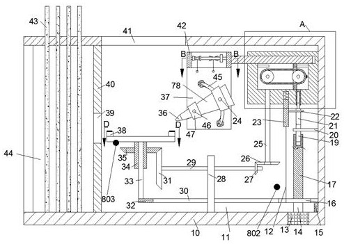
[0016] Combine below Figure 1-6 The present invention is described in detail, and for convenience of description, the orientations mentioned below are now stipulated as follows: figure 1 The up, down, left, right, front and back directions of the projection relationship itself are consistent.

[0017] refer to Figure 1-6 According to an embodiment of the present invention, a dust removal device for a circuit board with soldered components includes a dust removal box 10, a dust removal chamber 11 is provided in the dust removal case 10, and the top wall of the dust removal chamber 11 runs through There is an inlet 41 for putting into the circuit board, the left end of the dust removal chamber 11 is provided with a partition 40, the partition 40 is provided with an air outlet 39, and the left side of the air outlet 39 is connected with a purification chamber 44, so The clean chamber 44 is provided with a dust-proof plate 43 which is gradually increased from right to left, an...


PUM


Abstract

The invention discloses a dedusting and deashing device for a circuit board welded with components. The dedusting and deashing device for the circuit board welded with the components comprises a dedusting box, wherein a dedusting cavity is formed in the dedusting box; an inlet for placing the circuit board penetrates through the top wall of the dedusting cavity; a partition plate is arranged at the left end of the dedusting cavity; an air outlet is formed on the partition plate; the left side of the air outlet communicates with a purification cavity; a dust isolation plate with a dust isolation degree which is gradually increased from right to left is arranged in the purification cavity; and a transmission box is fixedly arranged on the right wall of the dedusting cavity. The angle of a fan can be continuously changed, the circuit board can also rotate and blow air at different angles, and therefore a great and comprehensive dedusting effect is achieved; and meanwhile, the blown air containing dust can be greatly subjected to dust isolation treatment, so that the situation that when operation is carried out in a warehouse, the dust is accumulated on the circuit board again due to the problem of no air circulation after being discharged into the warehouse, is avoided, and the situation that the air is polluted by the dust during dedusting is also avoided.

Description

technical field [0001] The invention relates to the related technical field of circuit boards, in particular to a dust-removing device for circuit boards with soldered components. Background technique [0002] The circuit board can be called a printed circuit board or a printed circuit board, which is a circuit component that welds various circuits to a board; in addition to welding the circuit, various electronic components are also welded on the circuit board, and after welding, it may be necessary If it is placed for a long time, a lot of dust will often accumulate at this time, and the dust must be removed during use, otherwise it may cause the circuit board to be short-circuited and damaged, and the general method of dust removal is to manually hold a hair dryer against the circuit Board air blowing dust removal, this method is labor-intensive and the dust removal effect is not good, obviously it is not suitable for the dust removal operation of a large number of circui...

Claims


Application Information

Patent Timeline
Patent Type & Authority Applications(China)
IPC IPC(8): B08B5/02B08B13/00
CPCB08B5/02B08B5/023B08B13/00
Inventor 马西尚
Owner PUJIANG LECHENG ELECTRONICS TECH CO LTD
Why Eureka
Try Eureka