

Solder ball with coating, ball mounting method and packaging method
A technology of solder balls and coatings, which is applied in the direction of assembling printed circuits, printed circuits, and electrical components with electrical components, can solve problems such as low efficiency, achieve high efficiency, and simplify the implantation process.
- Summary
- Abstract
- Description
- Claims
- Application Information
AI Technical Summary
Problems solved by technology
Method used
Image

Examples
Embodiment Construction
[0037] The application will be further described in detail below in conjunction with the accompanying drawings and embodiments. It should be understood that the specific embodiments described here are only used to explain related inventions, rather than to limit the invention. It should also be noted that, for ease of description, only parts related to the invention are shown in the drawings.
[0038] It should be noted that, in the case of no conflict, the embodiments in the present application and the features in the embodiments can be combined with each other. The present application will be described in detail below with reference to the accompanying drawings and embodiments.
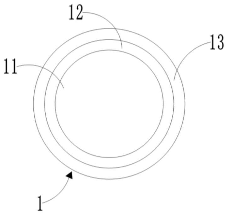
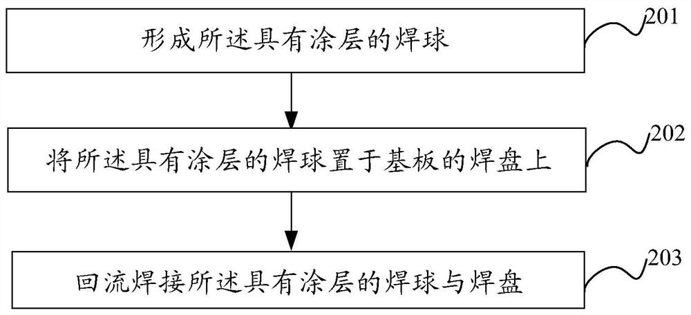
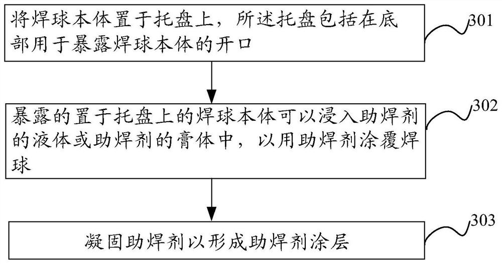
[0039] As mentioned in the background technology, the ball planting method of spot welding first and then reflow is relatively inefficient, and how to provide a more efficient ball planting method will become the improvement direction of this application. Therefore, the present application provide...
PUM
 Abstract
Description
Claims
Application Information