Bonding-free electronic tag chip packaging method
A label chip, packaging method technology, applied in the direction of circuits, electrical components, electrical solid devices, etc., can solve the problems of wrong chip placement, uneven dispensing, and reduced work efficiency.
- Summary
- Abstract
- Description
- Claims
- Application Information
AI Technical Summary
Problems solved by technology
Method used
Image
Examples
Embodiment approach
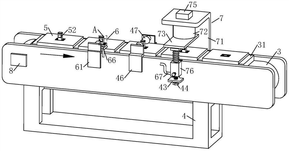
[0046] As an embodiment of the present invention, the bottom end of the chute 42 is fixedly connected to the limit plate 43, the shape of the end of the limit plate 43 close to the bracket 4 is consistent with the shape of the chute 42, and the middle part of the limit plate 43 is provided with a screw thread Hole, limiting plate 43 middle part is connected with adjusting screw 44 by screw thread, and the afterbody of described adjusting screw 44 is provided with gasket 45, and described gasket 45 is made of elastic material, and gasket 45 contacts with gas cylinder 76 bottom surfaces; During work, The amount of conductive glue injected by the dispensing module 6 into the base plate 5 depends on the expansion and contraction of the gas rod 77. Since the stroke of the positioning plate 73 is consistent each time, the amount of glue injected by the glue dispensing module 6 remains unchanged. All can affect the encapsulation quality of RFID chip 2 when being too much or too little...
PUM
 Abstract
Description
Claims
Application Information


