
Planarization method of IGBT device

A planarization method and device technology, applied in semiconductor devices, semiconductor/solid-state device manufacturing, electrical components, etc., can solve problems such as uniformity and adverse effects on performance of IGBT devices, large differences in wafer surface topography, etc., to avoid excessive Throwing and under-grinding, flush top surface, precise control effect

Pending Publication Date: 2020-12-15
BEIJING SEMICORE PRECISION MICROELECTRONICS EQUIP CO LTD
View PDF0 Cites 0 Cited by
  • Summary
  • Abstract
  • Description
  • Claims
  • Application Information

AI Technical Summary

Problems solved by technology

[0005] Therefore, the technical problem to be solved by the present invention is to overcome the defect that the existing IGBT device planarization process causes large shape differences on the wafer surface and adversely affects the uniformity and performance of the IGBT device in the wafer, thereby providing A planarization method for an IGBT device

Method used


Image

  • Planarization method of IGBT device
  • Planarization method of IGBT device
  • Planarization method of IGBT device

Examples


Embodiment 1

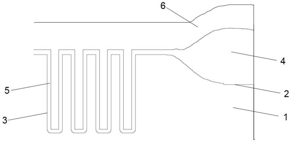
[0035] This embodiment provides a method for planarizing an IGBT device. Before the gate of the IGBT device is planarized, the structure of the gate of the IGBT device is as follows: figure 1 As shown: the substrate 1 includes a first trench 2 and several second trenches 3, and the depth of the second trench 3 is greater than that of the first trench 2, and a first insulating layer 4 is formed in the first trench 2 and the second trench The thickness of an insulating layer 4 is higher than the depth of the first trench 2, the bottom and side walls of the first trench 2 are formed with a second insulating layer 5, and the first insulating layer 4 communicates with the second insulating layer 5; the first A polysilicon layer 6 is formed on the insulating layer 4 and the second insulating layer 5, and the polysilicon layer 6 on the second insulating layer 5 extends to the outlet of the second groove 3. The material of the first insulating layer 4 and the second insulating layer 5 ...

Embodiment 2

[0042] This embodiment provides a method for planarizing an IGBT device. Before the gate of the IGBT device is planarized, the structure of the gate of the IGBT device is as follows: figure 1 As shown: the substrate 1 includes a first trench 2 and several second trenches 3, and the depth of the second trench 3 is greater than that of the first trench 2, and a first insulating layer 4 is formed in the first trench 2 and the second trench The thickness of an insulating layer 4 is higher than the depth of the first trench 2, the bottom and side walls of the first trench 2 are formed with a second insulating layer 5, and the first insulating layer 4 communicates with the second insulating layer 5; the first A polysilicon layer 6 is formed on the insulating layer 4 and the second insulating layer 5, and the polysilicon layer 6 on the second insulating layer 5 extends to the outlet of the second groove 3. The material of the first insulating layer 4 and the second insulating layer 5 ...

Embodiment 3

[0049] This embodiment provides a method for planarizing an IGBT device. Before the gate of the IGBT device is planarized, the structure of the gate of the IGBT device is as follows: figure 1 As shown: the substrate 1 includes a first trench 2 and several second trenches 3, and the depth of the second trench 3 is greater than that of the first trench 2, and a first insulating layer 4 is formed in the first trench 2 and the second trench The thickness of an insulating layer 4 is higher than the depth of the first trench 2, the bottom and side walls of the first trench 2 are formed with a second insulating layer 5, and the first insulating layer 4 communicates with the second insulating layer 5; the first A polysilicon layer 6 is formed on the insulating layer 4 and the second insulating layer 5, and the polysilicon layer 6 on the second insulating layer 5 extends to the outlet of the second groove 3. The material of the first insulating layer 4 and the second insulating layer 5 ...


PUM

PropertyMeasurementUnit
Diameteraaaaaaaaaa

Abstract

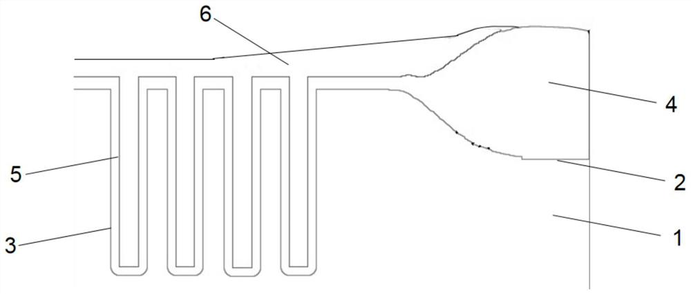
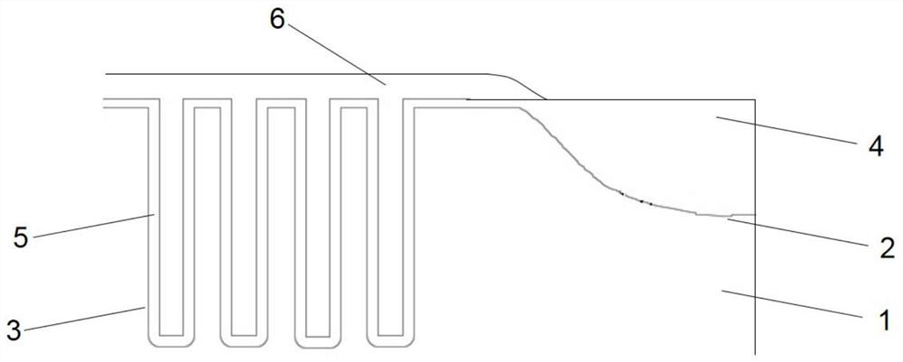
The invention provides a planarization method of an IGBT (Insulated Gate Bipolar Transistor) device. The method comprises the following steps of firstly, removing part of polycrystalline silicon through first grinding to expose a first insulating layer, and then, mainly removing part of the first insulating layer through second grinding to be flush with the upper surface of a second insulating layer, then, polycrystalline silicon on the upper surface of the second insulating layer being mainly removed through third grinding to expose the second insulating layer, that is, targeted grinding being achieved in each grinding process, meanwhile, each grinding process being matched with an online end point detection method to achieve control over each grinding end point, situations of over-polishing and insufficient grinding are avoided, and production efficiency is improved. Therefore, it is guaranteed that the upper surfaces of the first insulating layer and the second insulating layer obtained after planarization processing are flush, and accurate control over the uniformity of the surface morphology of the wafer is achieved.

Description

technical field [0001] The invention relates to the technical field of semiconductors, in particular to a method for planarizing an IGBT device. Background technique [0002] IGBT (Insulated Gate Bipolar Transistor), also known as insulated gate bipolar transistor, is currently the most representative power electronic device. IGBT is a composite full-control-voltage-driven-power semiconductor device composed of BJT (bipolar junction transistor) and MOS (insulated gate field effect transistor). It has the characteristics of self-shutoff, so it has both BJT devices and The advantages of MOS devices, such as voltage-controlled switching, high operating frequency, simple drive control circuit, and bipolar conduction, etc. The IGBT device has the characteristics of self-shutoff, it can be regarded as a wire when it is turned on, and it can be regarded as an open circuit when it is turned off. The control area of ​​the IGBT device is the gate area, and the electrode attached to ...

Claims


Application Information

Patent Timeline
IPC IPC(8): H01L21/331H01L29/739
CPCH01L29/66325H01L29/7393Y02P70/50
Inventor 崔凯
Owner BEIJING SEMICORE PRECISION MICROELECTRONICS EQUIP CO LTD
Learn More