On-chip calibrator model and method of parameter determination in on-chip calibrator model

A technology for determining parameters and calibrating models, which is applied in the field of on-chip calibration part models and parameter determination in on-chip calibration part models, can solve problems such as calibration and test accuracy reduction, achieve calibration and measurement errors, and improve test accuracy Effect

Active Publication Date: 2020-12-18
THE 13TH RES INST OF CHINA ELECTRONICS TECH GRP CORP
View PDF6 Cites 4 Cited by
  • Summary
  • Abstract
  • Description
  • Claims
  • Application Information

AI Technical Summary

Problems solved by technology

[0003] In view of this, the embodiment of the present invention provides an on-chip calibration model and a method for determining parameters in the on-chip calibration model, aiming at solving the problem of using traditional measurement models to calibrate the on-chip test system in the prior art. and the problem of reduced test accuracy

Method used


Image

  • On-chip calibrator model and method of parameter determination in on-chip calibrator model
  • On-chip calibrator model and method of parameter determination in on-chip calibrator model
  • On-chip calibrator model and method of parameter determination in on-chip calibrator model

Examples


Embodiment Construction

[0054] In the following description, specific details such as specific system structures and technologies are presented for the purpose of illustration rather than limitation, so as to thoroughly understand the embodiments of the present invention. It will be apparent, however, to one skilled in the art that the invention may be practiced in other embodiments without these specific details. In other instances, detailed descriptions of well-known systems, devices, circuits, and methods are omitted so as not to obscure the description of the present invention with unnecessary detail.

[0055] In order to illustrate the technical solutions of the present invention, specific examples are used below to illustrate.

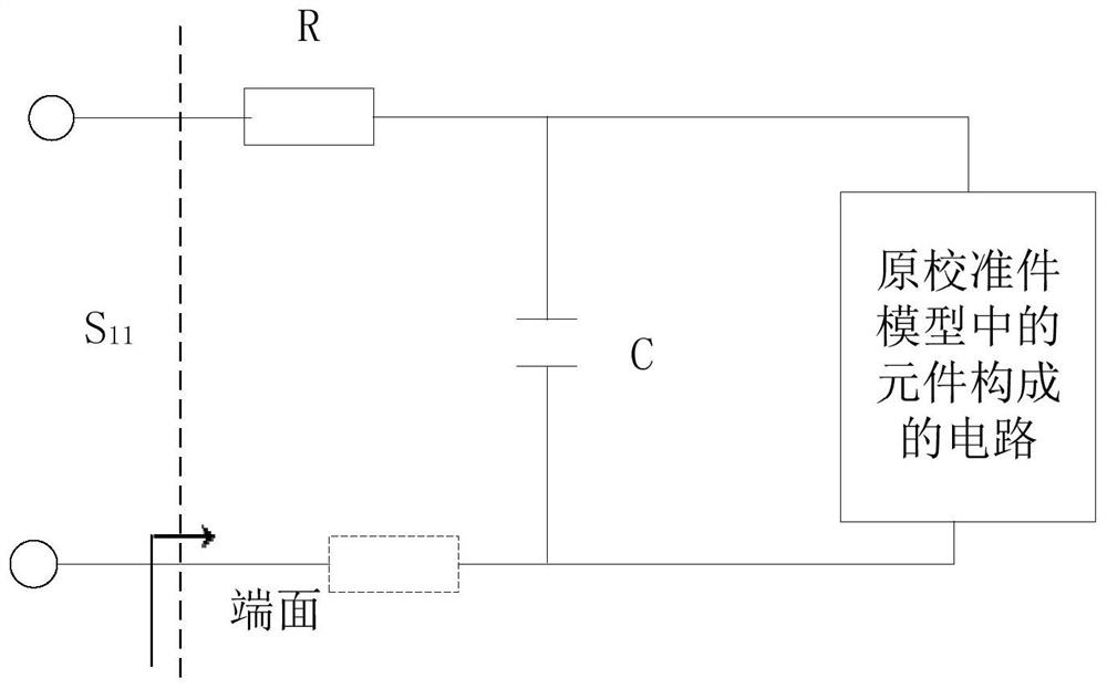
[0056] figure 1 A schematic diagram of an on-chip calibration object model provided for an embodiment of the present invention is described in detail as follows.

[0057] The on-chip calibration component model can include: the resistance representing the crosstalk of...


PUM


Abstract

The invention is applicable to the technical field of measurement of microwave characteristics of primary semiconductor devices, and provides an on-chip calibrator model and a method of parameter determination in the on-chip calibrator model. The on-chip calibration model comprises a resistor for representing crosstalk of an on-chip calibrator and a capacitor for representing crosstalk of the on-chip calibrator; the resistor representing crosstalk of the on-chip calibrator is connected in series with a circuit formed by elements in an original calibrator model, and one end of the capacitor representing crosstalk of the on-chip calibrator is connected between the resistor representing crosstalk of the on-chip calibrator and one end of the circuit formed by elements in the original calibrator model. And the other end of the capacitor representing crosstalk of the on-chip calibrator is connected to the other end of the circuit formed by the elements in the original calibrator model. According to the on-chip calibration model provided by the embodiment of the invention, the on-chip S parameter test accuracy of the terahertz frequency band can be improved.

Description

technical field [0001] The invention belongs to the technical field of microwave characteristic measurement of wafer-level semiconductor devices, and in particular relates to an on-chip calibration model and a method for determining parameters in the on-chip calibration model. Background technique [0002] "On-chip S-parameter test system" is widely used in the microelectronics industry. Before use, it is necessary to perform vector calibration on the on-chip S-parameter test system with the on-chip calibration kit. The accuracy of the calibration depends on the accuracy of the definition of the on-chip calibration kit. Different types of calibration kits (such as open calibration kits, short calibration kits, load calibration kits, and thru calibration kits) have different values ​​for the lumped parameters in the measurement model. Resistance, inductance, capacitance and DC resistance. How to obtain the accurate magnitude of each lumped parameter in the measurement model...

Claims


Application Information

Patent Timeline
Patent Type & Authority Applications(China)
IPC IPC(8): G01R31/26
CPCG01R31/2601
Inventor 王一帮吴爱华梁法国刘晨霍晔栾鹏孙静李彦丽
Owner THE 13TH RES INST OF CHINA ELECTRONICS TECH GRP CORP
Why Eureka
Try Eureka