Digital microscopic optical imaging device with long working distance
A working distance, digital microscopy technology, applied in the field of optical imaging, which can solve the problems of low resolution and short working distance of microscopes
- Summary
- Abstract
- Description
- Claims
- Application Information
AI Technical Summary
Problems solved by technology
Method used
Image
Examples
Embodiment
[0034] Optical structure design part:
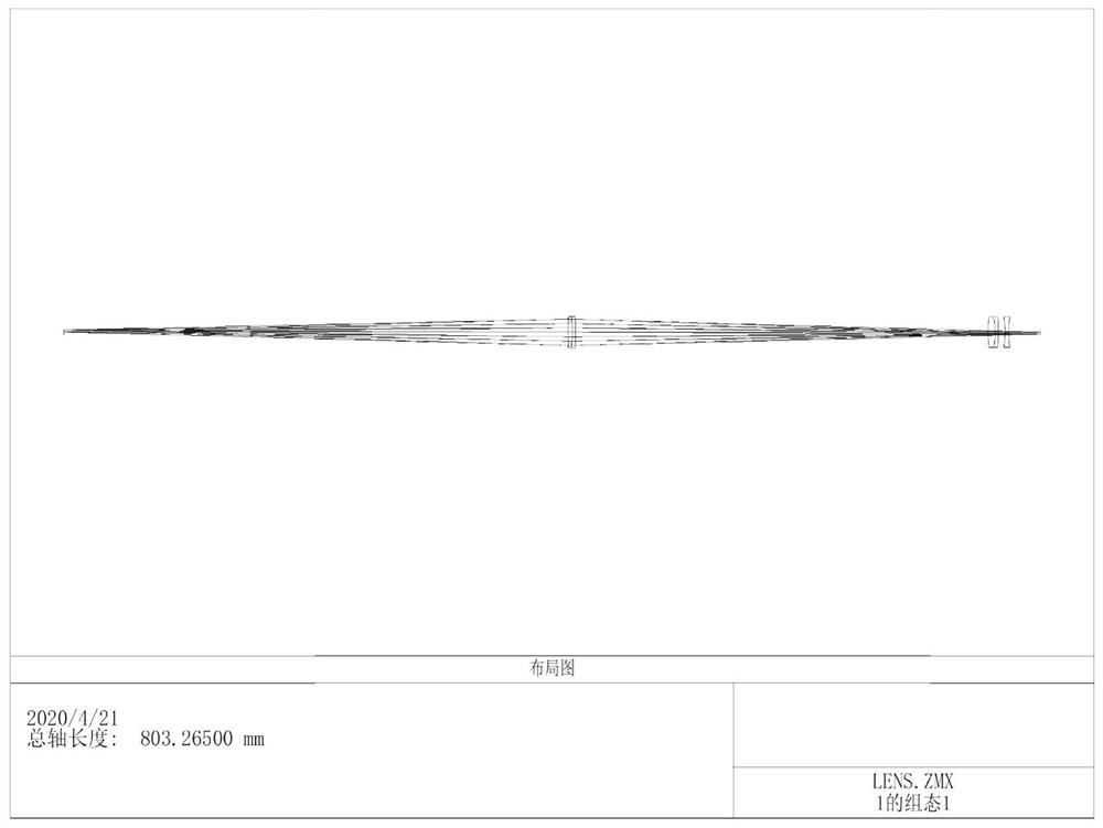
[0035] Please refer to figure 1 , the optical path diagram of the microscope lens assembly of the optical system, including a biconcave lens, an achromatic doublet convex lens 1, and a doublet convex lens 2 arranged on the main optical axis from right to left; wherein,
[0036] The diameter of the double-concave lens is 25.4 mm, made of BK7 material, and the center thickness is 3 ± 0.1 mm, and the edge thickness is 5 ± 0.1 mm;
[0037] The first lens and the second lens are achromatic lenses formed by bonding a positive lens and a negative lens;
[0038] The first diameter of the lens is 25.4mm, the biconvex is made of N-BK7 material, the meniscus is made of H-ZF2 material, the thickness of the center of the lens is 8.4±0.1mm, and the thickness of the edge is 6.85±0.1mm. The object plane is the positive meniscus of the negative lens, and the image plane is the positive meniscus of the positive lens.
[0039] The second diameter of the...
PUM
| Property | Measurement | Unit |
|---|---|---|
| thickness | aaaaa | aaaaa |
| thickness | aaaaa | aaaaa |
| thickness | aaaaa | aaaaa |
Abstract
Description
Claims
Application Information


