Optical modulation element

一种光调制元件、光调制层的技术,应用在光学元件、光学元件、光学部件等方向,能够解决产品品质劣化、表面弯曲等问题

一种光调制元件、光调制层的技术,应用在光学元件、光学元件、光学部件等方向,能够解决产品品质劣化、表面弯曲等问题

CN112105973AActive Publication Date: 2020-12-18LG CHEM LTD

Image

  • Optical modulation element
  • Optical modulation element
  • Optical modulation element

Examples


Embodiment 1

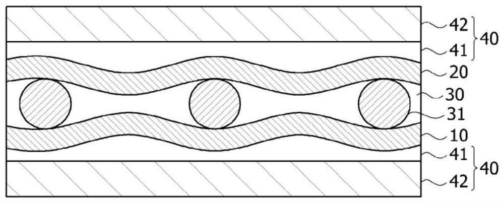
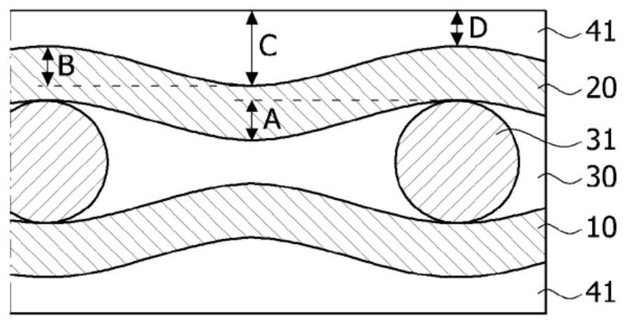
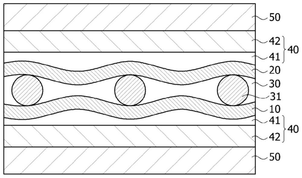
[0068] As the light modulation element of Example 1, a light modulation element having the shape of an eyewear lens was produced. Specifically, as a film having an electrode layer formed on each of the first base film and the second base film, a PC-ITO film (Teijin) having a total thickness of 100 μm was prepared in which the ITO layer was deposited on the PC film superior. A composition comprising a liquid crystal compound (MDA-16-1235, Merck) and a spherical spacer (KBN-512, Sekisui Co.) having a particle diameter of 12 μm was applied on the electrode layer of the first substrate film to form a light modulation layer . At this point, the composition was applied on the PC-ITO film in the inner region of the outer sealant applied in the shape of the edge of the eyewear lens. After the second base film is laminated so that the electrode layer of the second base film is in contact with the light modulation layer, due to the difference in force between the first base film and t...

Embodiment 2

[0070] A light modulation element was manufactured in the same manner as in Example 1 except that a TAC film (SHC40T190M, DAICEL) having a thickness of 190 μm in which a hard coat layer was formed on one side instead of the anti-fog layer was used.

Embodiment 3

[0072] A light modulation element was produced in the same manner as in Example 1, except that a PC film (OM81-5, Polyopt) having a thickness of 500 μm in which a hard coat layer was formed on one side was used instead of a hard coat layer formed on one side. TAC film with a thickness of 190 μm coated with an anti-fog layer.


PUM

PropertyMeasurementUnit
wavelengthaaaaaaaaaa
particle diameteraaaaaaaaaa

Abstract

The present application relates to an optical modulation element and a use thereof, and improves the surface waviness of a substrate film, which is caused by a spacer, so as to suppress a surface waviness phenomenon observed when the surface reflection is visually observed. The optical modulation element can be applied to various flexible display devices, thereby improving the quality of these products.

Description

technical field [0001] The present application relates to light modulating elements and their use. [0002] This application claims the benefit of priority based on Korean Patent Application No. 10-2018-0076481 filed on July 2, 2018 and Korean Patent Application No. 10-2019-0079555 filed on July 2, 2019, the disclosure of which Incorporated herein in its entirety by reference. Background technique [0003] In Patent Document 1 (Korean Patent Laid-Open No. 1775332), a light modulation element such as a liquid crystal cell may generally include a spacer to maintain a cell gap between an upper substrate film and a lower substrate film. In addition, when the light modulation element is applied to a strap-on flexible display device such as eyewear, flexible substrate films may be required for the upper and lower substrate films. [0004] However, when a flexible base film is applied to manufacture a light modulation element, there may arise a problem that, due to a difference i...

Claims


Application Information

Patent Timeline
18 Dec 2020
Publication
CN112105973A
IPC
G02B5/30; G02F1/35; B32B27/06; B32B3/28; B32B7/12
CPC
G02B1/18; G02B1/14; G02F1/133305; G02F1/1339; G02F1/13392; G02F1/13398; G02F1/13396; G02B5/305
Inventors
柳正善; 吴东铉