
Display panel, preparation method of display panel and display device

A display panel and display area technology, which is applied in the manufacture of semiconductor/solid state devices, semiconductor devices, electrical components, etc., can solve problems such as affecting the display effect of the display panel, uneven bright lines on the periphery of the display area, and misalignment of shading inks, etc. Achieve the effect of reducing the difficulty of preparation, optimizing the display effect, and ensuring stability

Active Publication Date: 2020-12-29
KUNSHAN GO VISIONOX OPTO ELECTRONICS CO LTD
View PDF3 Cites 1 Cited by
  • Summary
  • Abstract
  • Description
  • Claims
  • Application Information

AI Technical Summary

Problems solved by technology

[0004] However, there is a problem of alignment error in the application of light-shielding ink, which still cannot solve the problems of uneven display and bright lines around the display area, which affects the display effect of the display panel

Method used


Image

  • Display panel, preparation method of display panel and display device
  • Display panel, preparation method of display panel and display device
  • Display panel, preparation method of display panel and display device

Examples


Embodiment Construction

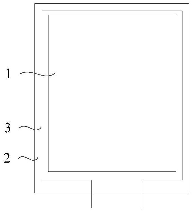
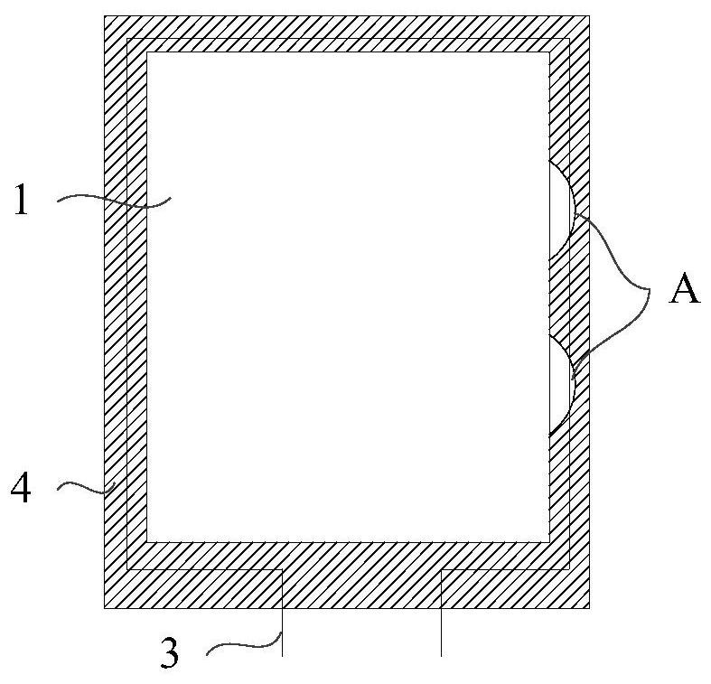
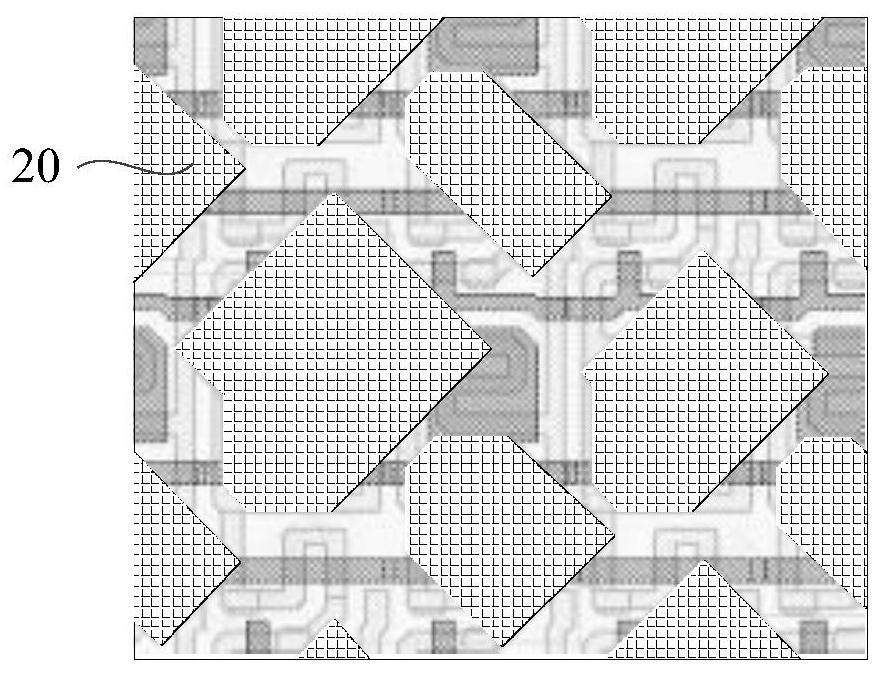
[0073] figure 1 It is a schematic diagram of the structure of the display panel. figure 2 It is a structural schematic diagram of a display panel coated with light-shielding ink in the prior art. image 3 It is a structural schematic diagram of a display area of ​​a display panel coated with light-shielding ink in the prior art. refer to Figure 1 to Figure 3 As shown, the current OLED is provided with a display area 1 and a non-display area 2 , and the non-display area 2 surrounds the periphery of the display area 1 . The cathode signal line set in the non-display area 2 and the ELVSS 3 signal line are overlapped through the anode signal line. Since the anode signal line is usually made of metal material containing silver, when the display panel is designed with a narrow frame structure, the distance between the anode signal line in the non-display area 2 and the display area 1 is reduced, and it is close to the anode signal line in the display area 1 It will be exposed,...


PUM


Abstract

The invention provides a display panel, a preparation method of the display panel and a display device. The display panel comprises a display area and a non-display area arranged on the periphery of the display area, an array substrate is arranged in the display area, a plurality of pixel areas are arranged on the array substrate in an array mode, and pixel limiting areas are formed between the adjacent pixel areas. Shading pieces are arranged in the pixel limiting areas. A shading part is arranged at the adjacent position of the display area and the non-display area, and at least part of theshading part extends into the non-display area. The problem that bright lines appear in the non-display area on the periphery of the display area can be avoided, meanwhile, reflective light is prevented from being generated in the display area, the stability of the characteristics of the thin film transistor in the display area is guaranteed, the contrast ratio and the black position level of thedisplay panel are improved, and the display effect of the display panel is optimized.

Description

technical field [0001] The present invention relates to the field of display technology, in particular to a display panel, a method for preparing the display panel and a display device. Background technique [0002] Organic Light-Emitting Diode (OLED) is a self-luminous device, because of its low power consumption, high color saturation, wide viewing angle, thin thickness, flexibility and no need for backlight, etc. With excellent performance, it is widely used in display devices such as terminal equipment and wearable equipment. [0003] The current OLED display panel is provided with a display area and a non-display area, and the non-display area surrounds the periphery of the display area. The cathode signal line and the ELVSS signal line arranged in the non-display area are overlapped by the anode signal line. Since the anode signal lines are usually made of metal materials containing silver, when the display panel is designed with a narrow frame structure, the distanc...

Claims


Application Information

Patent Timeline
IPC IPC(8): H01L27/32H01L51/56
CPCH10K59/126H10K59/122H10K71/00
Inventor 秦旭常苗张露胡思明
Owner KUNSHAN GO VISIONOX OPTO ELECTRONICS CO LTD
Learn More