Display screen, display device and preparation method of display screen

A technology of display screen and cathode layer, applied in semiconductor/solid-state device manufacturing, electrical components, electrical solid-state devices, etc., can solve the problems of increasing the light transmittance of the cathode layer, increasing the light diffraction rate, reducing the image effect, etc., so as to reduce the diffraction phenomenon, reduce light loss, improve the effect of image effects

Active Publication Date: 2021-01-08
YUNGU GUAN TECH CO LTD
View PDF6 Cites 3 Cited by
  • Summary
  • Abstract
  • Description
  • Claims
  • Application Information

AI Technical Summary

Problems solved by technology

[0004]Although the above method can increase the light transmittance of the cathode layer, correspondingly, it will also increase the diffraction rate of light and reduce the image captured by the photosensitive elements such as the camera under the screen Effect

Method used


Image

  • Display screen, display device and preparation method of display screen
  • Display screen, display device and preparation method of display screen
  • Display screen, display device and preparation method of display screen

Examples


Embodiment 2

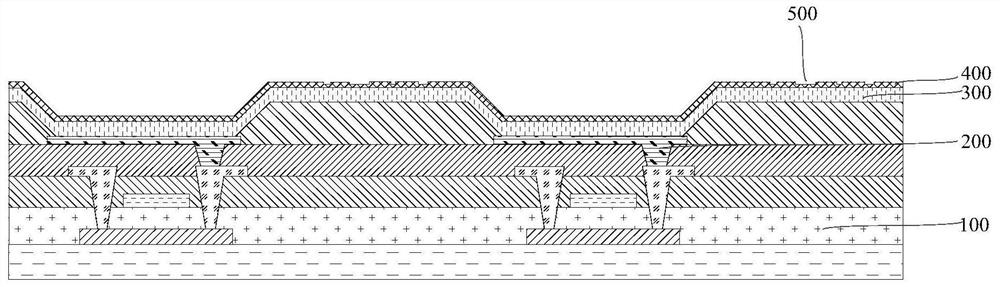
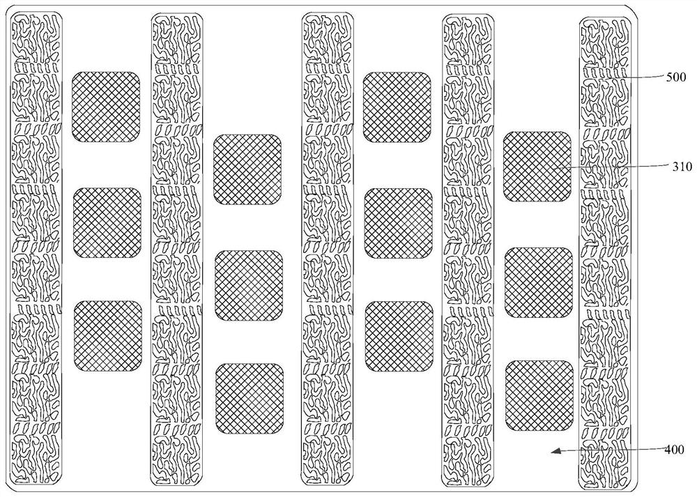
[0083] An embodiment of the present invention also provides a display device, including the display screen in the above embodiment and a photosensitive element located on the back of the display screen, wherein the hollow area 500 in the display screen corresponds to the photosensitive element.

[0084] Wherein, the display device can be applied to smart phones, tablet computers, notebook computers, and mobile terminals with display screens or other terminal devices. Photosensitive devices are cameras, sensors, and other devices with biometric recognition capabilities, which can be used for fingerprint recognition, palmprint recognition or face recognition.

[0085] Since the display device provided in this embodiment includes the display screen described in the above embodiment, the display device also has the same advantages as the above display screen. For details, please refer to related descriptions, which will not be repeated here.

[0086] In this embodiment, the cathod...

Embodiment 3

[0089] Such as Image 6 As shown, a method for preparing a display panel provided by an embodiment of the present invention includes the following steps:

[0090] S100: Provide an array substrate.

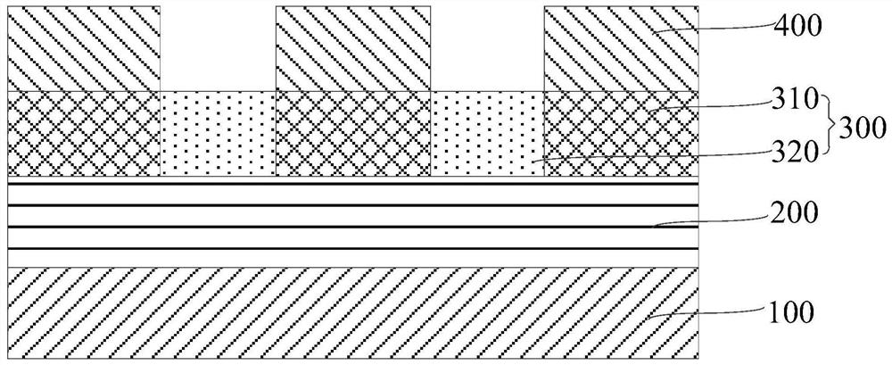
[0091]The array substrate 100 is used to carry other components of the display device, and to control current or voltage of other components disposed thereon. The array substrate 100 generally includes a substrate, a TFT array layer on the substrate and a planarization layer covering the TFT array layer.

[0092] S200: forming an anode layer on the array substrate.

[0093] The anode layer is formed on the planar layer of the array substrate by deposition, evaporation or sputtering; the anode layer generally includes a plurality of anode blocks arranged in an array, and each anode block passes through a via hole formed in the planarization layer Connect to source or drain in TFT array layer.

[0094] S300: Form a light emitting layer on the anode layer, the light emitting layer...


PUM


Abstract

The invention provides a display screen, a display device and a preparation method of the display screen, and relates to the technical field of display. The display screen comprises an array substrate, an anode layer, a light-emitting layer and a cathode layer which are stacked in sequence, wherein the light-emitting layer comprises a plurality of light-emitting units and pixel limiting layers forisolating the light-emitting units, the pixel limiting layer is a transparent layer, hollowed-out areas corresponding to the pixel limiting layers are arranged in the cathode layer, and the hollowed-out area is provided with a semi-light-transmitting part and a light-transmitting part penetrating through the cathode layer. According to the invention, the light transmittance of the cathode layer corresponding to the pixel limiting layer can be improved through the arrangement of the light transmission part, so that the image acquisition effect of the photosensitive element is improved; and thesemi-light-transmitting part ensures that when light emitted to the photosensitive element penetrates through the hollow area to greatly reduce the situation that the phase or the amplitude is too long, so that phase superposition can be avoided, the diffraction phenomenon is weakened, and the image effect obtained by the photosensitive element is further improved.

Description

technical field [0001] The invention relates to the field of display technology, in particular to a display screen, a display device and a preparation method of the display screen. Background technique [0002] With the rapid development of display technology, full-screen display has become a development trend of electronic devices such as mobile phones. In order to realize a full-screen display, it is usually necessary to arrange a camera under a display screen of an electronic device, thereby forming an under-screen camera. [0003] An OLED display usually includes an array substrate, an anode layer, a light-emitting layer, and a cathode layer stacked in sequence, wherein the light-emitting layer includes a plurality of light-emitting units and a pixel-defining layer for isolating each light-emitting unit. Since the pixel-defining layer does not emit light, therefore , in order to improve the light transmittance of the cathode layer, the portion of the cathode layer corre...

Claims


Application Information

Patent Timeline
Patent Type & Authority Applications(China)
IPC IPC(8): H01L51/52H01L51/56H01L27/32
CPCH10K59/122H10K50/822H10K50/828H10K71/00H10K71/621H10K59/80521H10K71/821H10K59/1201
Inventor 邢汝博刘如胜
Owner YUNGU GUAN TECH CO LTD
Why Eureka
Try Eureka