
LED module and display device

A technology of LED modules and LED chips, which is applied in the fields of nonlinear optics, instruments, optics, etc., and can solve problems such as the great influence on the signal integrity and reliability of LED chips, the high impedance of signal traces, and the impact on the luminous effect of LED chips, etc.

Active Publication Date: 2021-01-15
XIAMEN TIANMA MICRO ELECTRONICS
View PDF6 Cites 3 Cited by
  • Summary
  • Abstract
  • Description
  • Claims
  • Application Information

AI Technical Summary

Problems solved by technology

[0003] When the substrate of the LED module adopts a PCB board, since the PCB board mainly adopts the substrate material of the flame-resistant material grade FR4, due to the limitation of the process, the integration accuracy of the driver chip on the PCB board is low
When the substrate of the LED module uses a glass substrate, due to the limitation of the process, Mo / Al / Mo is usually used to form the signal wiring on the glass substrate. Due to the high resistivity of Al, the impedance of the signal wiring is too high, and the IR voltage is too high. The IR drop is large, which has a great impact on the integrity and reliability of the signal transmitted from the driver chip to the LED chip, and affects the luminous effect of the LED chip

Method used


Image

  • LED module and display device
  • LED module and display device
  • LED module and display device

Examples


Embodiment Construction

[0021] Various exemplary embodiments of the present invention will now be described in detail with reference to the accompanying drawings. It should be noted that the relative arrangements of components and steps, numerical expressions and numerical values ​​set forth in these embodiments do not limit the scope of the present invention unless specifically stated otherwise.

[0022] The following description of at least one exemplary embodiment is merely illustrative in nature and in no way taken as limiting the invention, its application or uses.

[0023] Techniques, methods and devices known to those of ordinary skill in the relevant art may not be discussed in detail, but where appropriate, such techniques, methods and devices should be considered part of the description.

[0024] In all examples shown and discussed herein, any specific values ​​should be construed as exemplary only, and not as limitations. Therefore, other instances of the exemplary embodiment may have dif...


PUM


Abstract

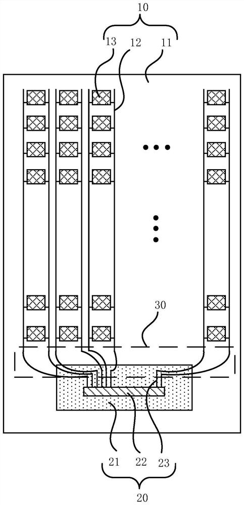
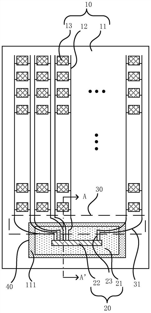
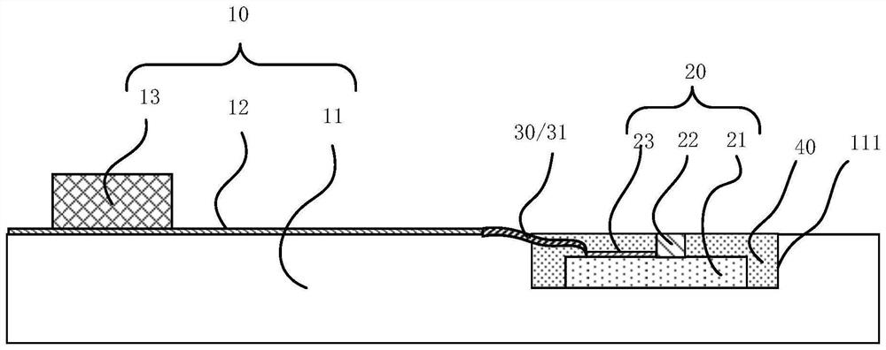
The invention discloses an LED module and a display device, and relates to the technical field of display, the LED module comprises an LED substrate, a driving substrate and a connecting structure; the LED substrate comprises a PCB substrate, a plurality of first signal wires and a plurality of LED chips arranged in an array, the LED chips and the first signal wires are arranged on the PCB substrate with the PCB substrate as a substrate, and first poles and second poles of the LED chips are connected with the different first signal wires respectively; the driving substrate comprises a glass substrate, a driving chip and a plurality of second signal wires, the driving chip and the second signal wires are arranged on the glass substrate by taking the glass substrate as a substrate, and one end of each second signal wire is electrically connected with the driving chip; and the first signal wire and the second signal wire are electrically connected through a connecting structure. Accordingto the invention, the IR voltage drop of the signal line between the driving chip and the LED chip can be effectively reduced while the integration precision of the driving chip is improved.

Description

technical field [0001] The present invention relates to the field of display technology, more specifically, to an LED module and a display device. Background technique [0002] Regional dimming technology is a hot spot in the current display field. As the regional dimming backlight module of the liquid crystal display panel, the light emitting diode (Light Emitting Diode, referred to as LED) module is the core device of the regional dimming display device, and the LED module The substrate generally adopts printed circuit board (Printed Circuit Board, referred to as PCB board) or glass substrate. and the signal routing between the driver chip. [0003] When the substrate of the LED module adopts a PCB board, since the PCB board mainly adopts the substrate material of flame-resistant material grade FR4, the integration precision of the driver chip on the PCB board is low due to the limitation of the process. When the substrate of the LED module uses a glass substrate, due to...

Claims


Application Information

Patent Timeline
IPC IPC(8): G02F1/13357
CPCG02F1/133603
Inventor 谢璐张学梅
Owner XIAMEN TIANMA MICRO ELECTRONICS
Learn More