System-on-chip supporting USB and GPIO conversion and communication method

A system-level chip and communication method technology, applied in general-purpose stored program computers, architectures with a single central processor, instruments, etc., can solve the problems of limiting user design flexibility and high cost, avoiding design complexity and reducing system. Power consumption and the effect of widening application scenarios

Active Publication Date: 2021-01-22
GOWIN SEMICON CORP LTD
View PDF4 Cites 0 Cited by
  • Summary
  • Abstract
  • Description
  • Claims
  • Application Information

AI Technical Summary

Problems solved by technology

[0003] For the system-on-chip based on FPGA and MCU design, in order to connect with different kinds of external devices, the system-on-chip needs to be configured with different types of interfaces, but if it is necessary to estab...

Method used


Image

  • System-on-chip supporting USB and GPIO conversion and communication method
  • System-on-chip supporting USB and GPIO conversion and communication method
  • System-on-chip supporting USB and GPIO conversion and communication method

Examples


Embodiment Construction

[0030] The system-on-a-chip supporting USB and GPIO conversion and the communication method of the present invention will be further described in detail below in conjunction with the accompanying drawings and specific embodiments. The advantages and features of the present invention will become clearer from the following description. It should be noted that all the drawings are in a very simplified form and use imprecise scales, and are only used to facilitate and clearly assist the purpose of illustrating the embodiments of the present invention.

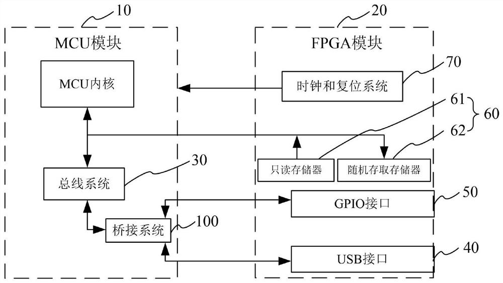
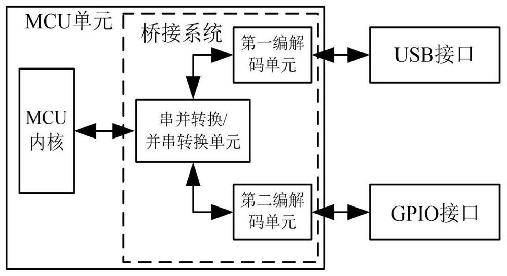
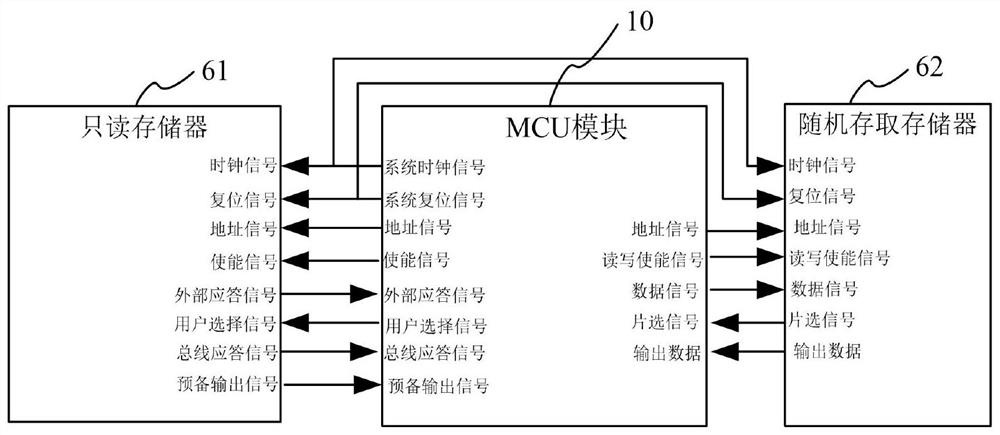
[0031] The embodiment of the present invention relates to a system-level chip supporting USB (Universal Serial Bus) and GPIO (General Input / Output Port) conversion. figure 1 It is a schematic structural diagram of a system-on-a-chip supporting USB and GPIO conversion according to an embodiment of the present invention. see figure 1 , the system level chip of the embodiment of the present invention is mainly based on MCU (microcon...


PUM


Abstract

The invention relates to a system-on-chip supporting USB and GPIO conversion and a communication method. The system-on-chip is integrated with an MCU (Microprogrammed Control Unit) module, an FPGA (Field Programmable Gate Array) module, a bus system, a USB (Universal Serial Bus) interface and a GPIO (General Purpose Input/Output) interface, wherein the USB interface and the GPIO interface are configured by utilizing hardware logic resources of the FPGA module, and the system-on-chip is also provided with a bridging system for connecting the USB interface and the GPIO interface. The system-on-chip gives consideration to the functions and advantages of an MCU and an FPGA, facilitates the meeting of diversified system functional requirements, avoids the design complexity caused by the use ofa USB-to-GPIO dedicated control chip through the setting of the bridging system, enables the design of a user to be more flexible, and is lower in cost. The method adopts the system-on-chip to carry out communication.

Description

technical field [0001] The invention relates to the field of FPGA application, in particular to a system-level chip supporting USB and GPIO conversion and a communication method. Background technique [0002] The function and performance of traditional FPGA (Field Programmable Gate Array, field programmable gate array) and CPU (central processing unit) discrete devices are increasingly difficult to meet the increasingly large and diverse data processing requirements. In order to meet the requirements of performance, scalability and integration Requirements, the industry has proposed a system-on-a-chip (SoC, also called system-on-chip) architecture based on FPGA and MCU (Micro-controller Unit, microcontroller) that integrates the advantages of FPGA and CPU. MCU (microcontroller) usually focuses on the number of I / O interfaces and the size of programmable memory, which is suitable for a large number of input and output (I / O) operations, but its processing power and I / O resourc...

Claims


Application Information

Patent Timeline
IPC IPC(8): G06F13/42G06F15/78
CPCG06F13/4282G06F15/7807G06F2213/0038G06F2213/0042
Inventor 赵井坤赵方亮崔明章孙莉莉贾瑞华
Owner GOWIN SEMICON CORP LTD
Why Eureka
Try Eureka