Chip sintering method and device, electronic equipment and readable storage medium

A sintering device and chip technology, which is applied in the manufacturing of circuits, electrical components, semiconductor/solid-state devices, etc., can solve the problems of not considering the pressing speed and pressing height of the nozzle, reducing the sintering accuracy of the chip, and the collision offset of the chip.

Pending Publication Date: 2021-01-22
ZHEJIANG RECI LASER TECH CO LTD
View PDF0 Cites 0 Cited by
  • Summary
  • Abstract
  • Description
  • Claims
  • Application Information

AI Technical Summary

Problems solved by technology

[0003] At present, most chip sintering methods use the suction nozzle to absorb the chip and heat sink in the material box, and directly attach the chip to the heat sink in the solder area for sintering. This process does not consider the spee...

Method used


Image

  • Chip sintering method and device, electronic equipment and readable storage medium
  • Chip sintering method and device, electronic equipment and readable storage medium
  • Chip sintering method and device, electronic equipment and readable storage medium

Examples


Embodiment Construction

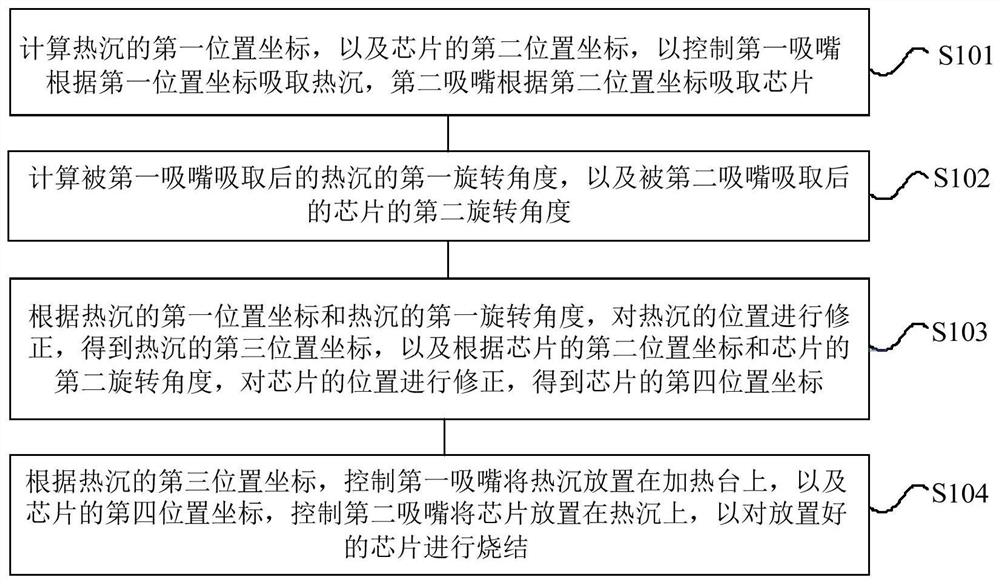
[0030] In order to make the purpose, technical solutions and advantages of the embodiments of the present application clearer, the technical solutions in the embodiments of the present application will be clearly and completely described below in conjunction with the drawings in the embodiments of the present application. Obviously, the described embodiments are only It is a part of the embodiments of this application, not all of them. The components of the embodiments of the application generally described and illustrated in the figures herein may be arranged and designed in a variety of different configurations. Accordingly, the following detailed description of the embodiments of the application provided in the accompanying drawings is not intended to limit the scope of the claimed application, but merely represents selected embodiments of the application. Based on the embodiments of the present application, all other embodiments obtained by those skilled in the art without...


PUM


Abstract

The invention provides a chip sintering method and device, electronic equipment and a readable storage medium. The method comprises the steps of: calculating a first position coordinate of a heat sinkand a second position coordinate of a chip so as to control a first suction nozzle to suck the heat sink according to the first position coordinate and control a second suction nozzle to suck the chip according to the second position coordinate, calculating a first rotation angle of the heat sink sucked by the first suction nozzle and a second rotation angle of the chip sucked by the second suction nozzle; correcting the first position coordinate of the heat sink and correcting the second position coordinate of the chip; and according to a corrected third position coordinate of the chip and acorrected fourth position coordinate of the heat sink, placing the heat sink on a heating table, and placing the chip on the heat sink so as to sinter the placed chip. Collision and deviation generated in the positioning process and displacement of the chip position in the welding process can be avoided, and the sintering precision is improved.

Description

technical field [0001] The present application relates to the technical field of semiconductors, in particular to a chip sintering method, device, electronic equipment and readable storage medium. Background technique [0002] At present, due to the high cost of chip production, the effect of chip sintering directly affects the pass rate of chip production in the process of chip sintering, so low-cost and high-precision sintering methods are particularly important. [0003] Most of the current chip sintering methods use the suction nozzle to absorb the chip and heat sink in the material box, and directly attach the chip to the heat sink in the solder area for sintering. This process does not consider the speed and height of the suction nozzle. , causing the nozzle to collide with the chip and the heat sink during the high-speed pressing process, and the position of the chip shifts during the welding process, thereby reducing the chip sintering accuracy. Contents of the inv...

Claims


Application Information

Patent Timeline
IPC IPC(8): H01L21/324H01L21/67
CPCH01L21/324H01L21/67259
Inventor 马进任杰席中秋牛奔刘江马海柱
Owner ZHEJIANG RECI LASER TECH CO LTD
Why Eureka
Try Eureka