
Electronic product chip detection equipment

A technology for chip detection and electronic products, which is applied in the direction of measuring electricity, measuring devices, measuring electrical variables, etc., can solve the problems of not being able to detect chips and keep picking and placing chips, and achieve the effect of improving work efficiency

Inactive Publication Date: 2021-01-26
江西国丰电子科技有限公司
View PDF1 Cites 3 Cited by
  • Summary
  • Abstract
  • Description
  • Claims
  • Application Information

AI Technical Summary

Problems solved by technology

[0005] In order to overcome the shortcomings of the current way of detecting chips that cannot detect chips in large quantities and need to pick and place chips continuously, the technical problem to be solved is to provide a method that can automatically detect chips and quickly detect chips. Placed electronic product chip testing equipment

Method used


Image

  • Electronic product chip detection equipment
  • Electronic product chip detection equipment
  • Electronic product chip detection equipment

Examples


Embodiment 1

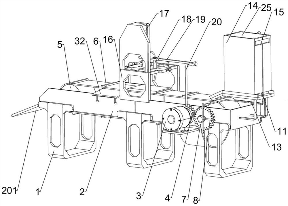
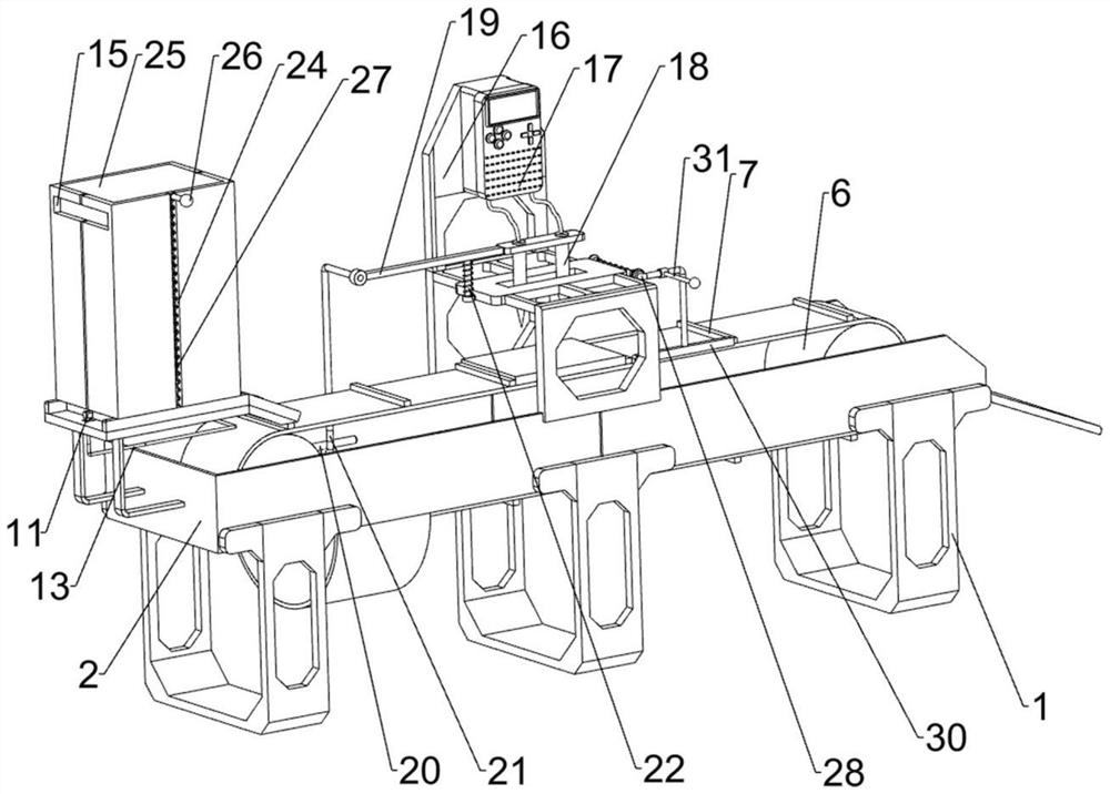
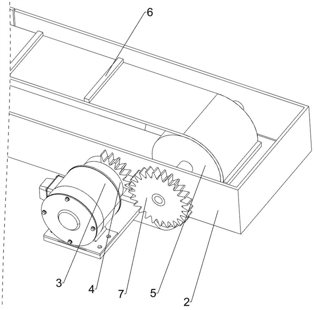
[0023] A chip testing equipment for electronic products, such as Figure 1-Figure 5 As shown, it includes a frame 1, a drive assembly, a blanking assembly and a detection assembly. The frame 1 is used to install the entire device. The top of the frame 1 is provided with a drive assembly that provides power for transmission. The unloading assembly is used for unloading by means of the drive assembly, and the detection assembly for detection by contact is installed in the middle of the drive assembly.

[0024] When it is necessary to perform quality inspection on the chip, the staff will place a certain amount of chips in the blanking assembly, and then start the drive assembly to transfer the chips in the blanking assembly. When the chip is moved to a certain position, the chip stops moving, and at the same time , the testing component performs quality testing on the chip, and after all the chips are tested, the staff can turn off the driving component.

[0025] Such as Figu...

Embodiment 2

[0032] On the basis of Example 1, such as figure 1 , figure 2 and Figure 4Shown, also include the first push plate 25, handle 26 and the 3rd spring 27, have the second through hole 24 at the rear portion of the blanking frame 14, the sliding type is provided with the first push plate 25 in the blanking frame 14, the second A handle 26 is welded on the rear side of a push plate 25 , and the handle 26 is slidably connected to the second through hole 24 , and a third spring 27 is connected between the handle 26 and the blanking frame 14 .

[0033] When it is necessary to put chips into the blanking frame 14, pull the handle 26 to slide upwards, and the third spring 27 stretches to drive the first push plate 25 to slide upwards. When a certain amount of chips are put into the blanking frame 14, Unclamp the handle 26, and under the action of the third spring 27, the handle 26 and its upper device are driven to move downwards to push and fix the chips. In this way, chips with po...


PUM


Abstract

The invention relates to chip detection equipment, in particular to electronic product chip detection equipment. The electronic product chip detection equipment provided by the invention can automatically detect a chip and rapidly place the chip. The electronic product chip detection equipment comprises a frame used for installing the whole device; a driving assembly, mounted on the rack and provides power for transmission; a discharging assembly, installed on the driving assembly and conducting discharging in a sliding mode; and a detection assembly, installed on the driving assembly and carrying out detection in a contact mode. Through cooperation of the transmission belt and the push block, a chip can be automatically transmitted, the working efficiency is improved, through cooperationof the first push rod and the contact rod, the chip can be automatically discharged, manual placement is not needed, and through cooperation of the detection pen and the second push rod, the chip canbe automatically detected.

Description

technical field [0001] The invention relates to a chip detection device, in particular to an electronic product chip detection device. Background technique [0002] Chips, also known as microcircuits, microchips, and integrated circuits, refer to silicon chips containing integrated circuits. They are small in size and are often part of computers or other electronic equipment. After the chip is manufactured, it is necessary to perform a resistance test on the chip. . [0003] Patent Publication No. CN208953668U discloses a portable commonly used chip detector, which includes a microprocessor IAP15F2K61S2, a digital chip detection module, an analog chip detection module, a time-based chip detection module, a three-terminal voltage regulator chip detection module, and a display module , detection operation module, alarm reminder module and power supply module. The microprocessor IAP15F2K61S2 controls and detects the IO port connected to the digital chip detection module, and ...

Claims


Application Information

Patent Timeline
Patent Type & Authority Applications(China)
IPC IPC(8): G01R31/01
CPCG01R31/01
Inventor 周丽建
Owner 江西国丰电子科技有限公司
Learn More