PCB defect detection method based on boundary segment number values

A defect detection and boundary technology, applied in image data processing, instruments, calculations, etc., can solve the problems of long time consumption, poor precision, and no further accurate determination of circuit boards

Pending Publication Date: 2021-01-29
FOSHAN NANHAI GUANGDONG TECH UNIV CNC EQUIP COOP INNOVATION INST +1
View PDF0 Cites 1 Cited by
  • Summary
  • Abstract
  • Description
  • Claims
  • Application Information

AI Technical Summary

Problems solved by technology

[0003] Due to technical reasons, most manufacturers still use manual detection methods, and the manual detection methods have the following problems: (1) The subjective evaluation has a great influence, the detection standards vary from person to person, and the detection efficiency is low, especially for high-precision It takes a long time and the accuracy is poor; (2) It can only preliminarily judge whether there is a defect, and does not further accurately determine which type of defect it is

Method used


Image

  • PCB defect detection method based on boundary segment number values
  • PCB defect detection method based on boundary segment number values
  • PCB defect detection method based on boundary segment number values

Examples


Embodiment approach

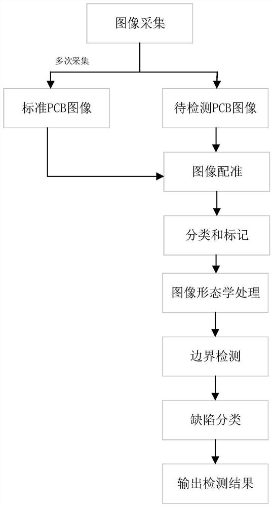
[0072] As a preferred embodiment of the present invention, the step S4 specifically includes:

[0073] S401. Use the method of morphological closed operation to eliminate the noise in the image of the printed circuit board to be tested. Specifically, perform the expansion operation first, specifically: translate the structural element B by a to obtain B a , if B a When X is hit, point a is recorded, and the expansion operation is as follows:

[0074]

[0075] Among them, X is the object to be processed, and B is the structural element;

[0076] Specifically, the processed object refers to the image of the printed circuit board to be tested;

[0077] S402. Carry out the corrosion operation again, and use B to corrode X to obtain a set, which is the set of the origin position of S when B is completely included in X, and the corrosion operation is as follows:

[0078]

[0079] Specifically, the S refers to the pixels in the image of the printed circuit board to be tested...


PUM


Abstract

The invention discloses a PCB defect detection method based on boundary segment number values, and the method comprises the following steps: S1, employing a plurality of standard images, obtaining thestandard images through an averaging method, carrying out the repeated image collection of a standard printed circuit board, and calculating to obtain a gray scale average value, and obtaining a standard printed circuit board image; s2, performing image registration on the image of the printed circuit board to be detected; s3, classifying and marking the images of the printed circuit board to bedetected by adopting a refining operation and a trimming operation; and S4, performing morphological operation on the image of the printed circuit board to be detected by adopting a morphological closed operation method so as to eliminate noise in the image, and the like. The method can replace a traditional manual visual inspection method, and achieves the purpose of saving the manufacturing costof the PCB by improving the PCB defect recognition efficiency and reducing the time consumed by a detection process.

Description

technical field [0001] The invention relates to the technical field of automatic visual inspection, in particular to a method for detecting PCB defects based on the number of boundary segments. Background technique [0002] Printed Circuit Board (PCB for short) is a vital electronic component in modern electronic products. As the layout of PCB becomes more and more compact, the smaller conductive path width and spacing make it more difficult to detect defects, and PCB defect detection is a challenge that PCB manufacturers must overcome in their product quality control, and it is an inevitable production in the industry. process flow. Therefore, detecting defects on PCBs quickly and accurately has become an urgent problem for PCB manufacturers. [0003] Due to technical reasons, most manufacturers still use manual detection methods, but the manual detection methods have the following problems: (1) The subjective evaluation has a great influence, the detection standards vary...

Claims


Application Information

Patent Timeline
Patent Type & Authority Applications(China)
IPC IPC(8): G06T7/30G06T7/155G06T7/13G06T7/00G06T5/30G06T5/00
CPCG06T5/002G06T5/30G06T7/0004G06T2207/30141G06T7/13G06T7/155G06T7/30
Inventor 陈强朱涛王华龙杨海东
Owner FOSHAN NANHAI GUANGDONG TECH UNIV CNC EQUIP COOP INNOVATION INST
Why Eureka
Try Eureka