Apparatus for simultaneously transferring micro-devices to target object

A micro-device and target technology, applied in the direction of electrical solid-state devices, semiconductor devices, semiconductor/solid-state device manufacturing, etc., can solve problems such as horizontal contact or uneven adhesion, and lower transfer yield

Pending Publication Date: 2021-01-29
兰蒂斯有限公司
View PDF0 Cites 1 Cited by
  • Summary
  • Abstract
  • Description
  • Claims
  • Application Information

AI Technical Summary

Problems solved by technology

That is, transfer yield may be reduced due to slight irregular horizontal contact or uneven adhesion in the sheet

Method used


Image

  • Apparatus for simultaneously transferring micro-devices to target object
  • Apparatus for simultaneously transferring micro-devices to target object
  • Apparatus for simultaneously transferring micro-devices to target object

Examples


Embodiment Construction

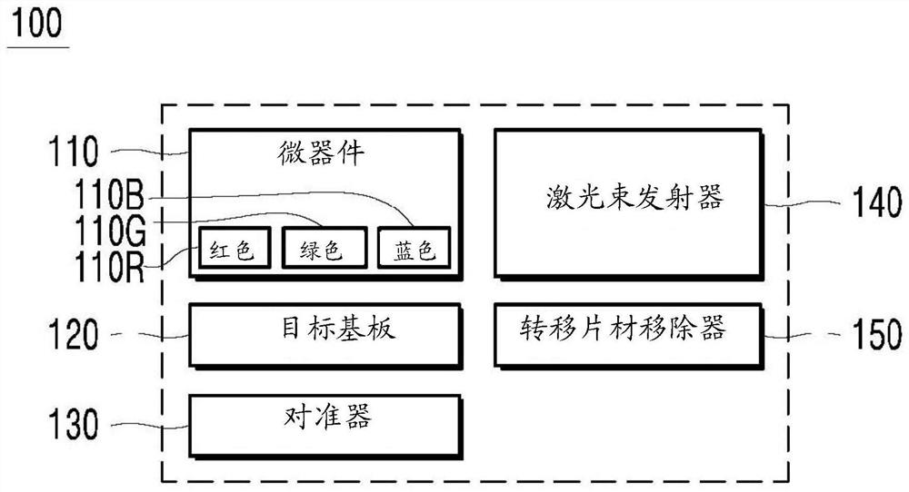
[0026] Hereinafter, preferred embodiments of the present application will be described in detail with reference to the accompanying drawings in order to easily understand the configuration and effects of the present application. For the purpose of clarity, not all details of known functions or components in this specification will be described in detail if it is deemed that such details may unnecessarily obscure the gist of the application.

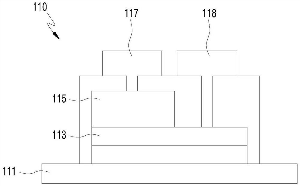
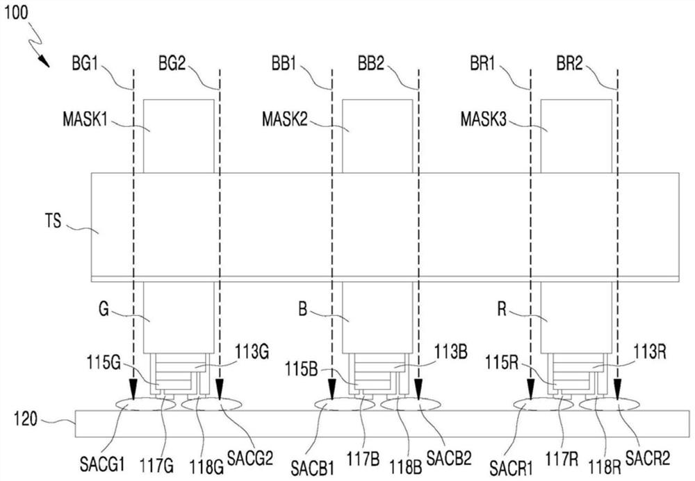
[0027] Before starting the description with reference to the accompanying drawings, the term "micro device" as used herein may refer to a specific device or structure of descriptive dimensions according to an embodiment of the present application. As used herein, "microdevice" may be used to refer to a structure or device having dimensions on the order of 1 μm to 500 μm. In particular, the microdevices may have a width or length in the range of 1 to 50 microns, 50 to 500 microns, or 10 to 250 microns. The thickness of a micro-device is u...


PUM

PropertyMeasurementUnit
thicknessaaaaaaaaaa
transmittivityaaaaaaaaaa

Abstract

Disclosed is an apparatus for simultaneously transferring micro-devices to a target object. The apparatus may comprise: multiple red (R), green (G), and blue (B) micro-devices attached to a carrier sheet by an adhesive material; a target substrate to which the micro-devices are transferred; an alignment unit for aligning the multiple micro-devices with the substrate; and a laser beam unit disposedabove the carrier sheet so as to emit a beam having a specific wavelength in the direction passing through the carrier sheet, wherein the micro-devices each comprise: a growth substrate; a first semiconductor layer and a second semiconductor layer disposed on the growth substrate; a first pad disposed on the first semiconductor layer; a second pad disposed on the second semiconductor layer; and an adhesive material disposed on the first pad and the second pad, and when the micro-devices and the substrate are aligned in transfer positions by the alignment unit, the laser beam unit applies energy to the adhesive material so as to allow the micro-devices to be transferred to the substrate. Accordingly, the efficiency of transfer can be improved.

Description

technical field [0001] The present application relates to a device for the simultaneous transfer of microdevices to a target object. Background technique [0002] Stamp transfer refers to a transfer in which an item to be transferred (for example, a microdevice) is mounted on a substrate, and since the contact surface between the microdevice and the substrate is flat, the level of the two contact surfaces Alignment is important, and the adhesion between the micro-device and the sheet is an important factor for transfer. That is, transfer yield may be lowered due to slight irregular horizontal contact or unevenness in adhesive force in the sheet. [0003] Therefore, when transferring a micro device to a substrate, a transfer method with excellent transfer efficiency is required. In addition, a transfer method for transferring a large number of microdevices included in a large area to a substrate is required. [0004] The above information is presented as background informa...

Claims


Application Information

Patent Timeline
Patent Type & Authority Applications(China)
IPC IPC(8): H01L21/67H01L21/68H01L21/52
CPCH01L2224/81H01L2933/0066H01L25/0753H01L33/62H01L21/67144H01L21/6835H01L2221/68322H01L2221/68354H01L2221/68381H01L21/52H01L21/67092H01L21/68H01L2221/68368
Inventor 安重仁安道焕
Owner 兰蒂斯有限公司
Why Eureka
Try Eureka