Method and circuit for pre-charging memory array and memory chip

A memory array and pre-charging circuit technology, applied in static memory, read-only memory, information storage, etc., can solve the problems of slow pre-charging, affecting costs, and occupying a large wafer area, so as to improve read speed and save costs Effect

Pending Publication Date: 2021-02-23
深圳爱思存储科技有限公司
View PDF1 Cites 0 Cited by
  • Summary
  • Abstract
  • Description
  • Claims
  • Application Information

AI Technical Summary

Problems solved by technology

[0003] In the patent No. US6175523, each row of bit lines has its own pre-charging circuit, which has the following defects. Each row has a pre-charging circuit, which occupies a large area of ​​the wafer and affects the cost; pre-charging is relatively slow, for NAND flash memory, because There will be a large parasitic capacitance on the bit line, and the pre-charging time often exceeds 5 microseconds, coupled with the uneven production process, often the pre-charging will be even slower

Method used


Image

  • Method and circuit for pre-charging memory array and memory chip
  • Method and circuit for pre-charging memory array and memory chip

Examples


Embodiment Construction

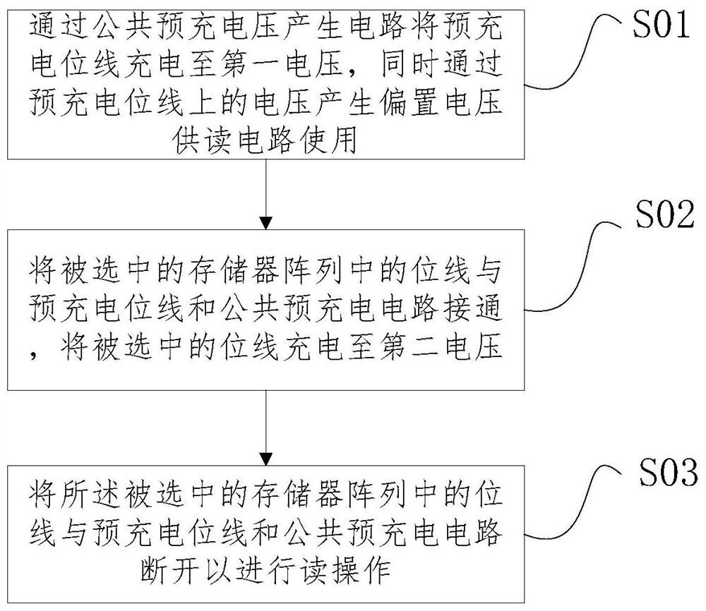
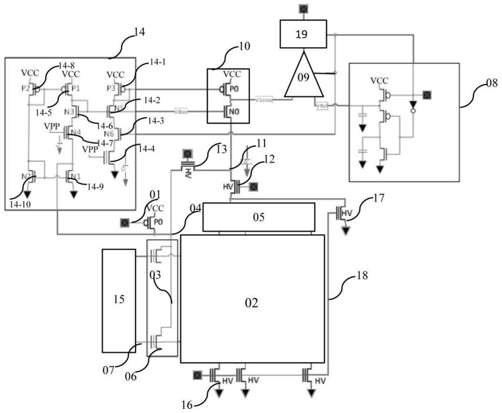
[0017] In order to enable those skilled in the art to better understand the solution of the present application, the technical solution in the embodiment of the application will be clearly and completely described below in conjunction with the accompanying drawings in the embodiment of the application. Obviously, the described embodiment is only It is an embodiment of a part of the application, but not all of the embodiments. Based on the embodiments in this application, all other embodiments obtained by persons of ordinary skill in the art without creative efforts shall fall within the scope of protection of this application.

[0018] In this application, the specific memory array is a NAND memory array, and it can also be other memory arrays. The specific embodiment will be described in detail by taking the NAND memory array as an example, because NAND is a structure well known to those skilled in the art, and will not be repeated here. , the specific charging process and re...


PUM


Abstract

The embodiment of the invention provides a method and a circuit for pre-charging a memory bit line during reading operation and a memory chip, and the whole memory array can share a pre-charging circuit by adding a pre-charging bit line in the memory array to assist pre-charging, so that the cost is saved, the pre-charging speed is doubled, and the pre-charging efficiency is improved. Therefore, the reading speed is improved.

Description

technical field [0001] The various embodiments of the present application belong to the field of storage devices, and in particular relate to a method, circuit and memory chip for precharging a memory array. Background technique [0002] In the memory, precharging the bit line is a commonly used method to increase the read speed. Generally, a differential amplifier is used to generate the read result. Before the read operation is sampled, the bit line connected to the signal input terminal and the reference terminal are precharged to the power supply voltage. Half, and then turn on the memory cells on a certain row, the memory cells in different states will increase the bit line voltage or reduce the bit line voltage, and then the differential amplifier starts to sample the output results. This method is a relatively standard operation in NAND memory. [0003] In the patent No. US6175523, each column bit line has its own pre-charging circuit, which has the following defects....

Claims


Application Information

Patent Timeline
IPC IPC(8): G11C16/24G11C16/30G11C16/04
CPCG11C16/0483G11C16/24G11C16/30
Inventor 托西德拉扎苏兹尔詹铃木瑞恩
Owner 深圳爱思存储科技有限公司
Why Eureka
Try Eureka