Wafer pre-aligner and method of pre-aligning wafer
A pre-alignment, wafer technology, applied in the direction of instrumentation, scientific instrumentation, semiconductor/solid-state device manufacturing, etc.
- Summary
- Abstract
- Description
- Claims
- Application Information
AI Technical Summary
Problems solved by technology
Method used
Image

Examples
Embodiment Construction
[0023] Embodiments of the present invention will be described below with reference to the drawings. In the following description, constituent elements having substantially the same function and arrangement are denoted by the same reference numerals, and description is repeated only when necessary.
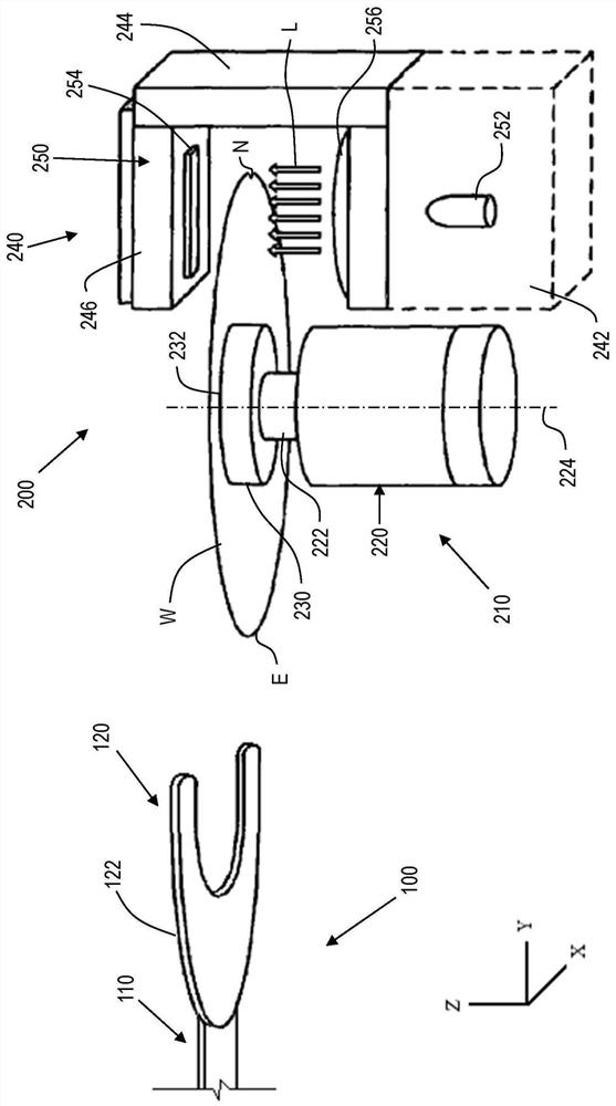
[0024] In semiconductor manufacturing, it is important to accurately determine the position (ie, position and orientation) of a semiconductor wafer in order to accurately perform a precise manufacturing process on the semiconductor wafer. Determining the position of a semiconductor wafer in certain processing stations is important as the wafers are moved from processing station to processing station, for example by using a robot such as an atmospheric articulated robot. For example, a pre-aligner may be used to identify the location of the indentations on the periphery of the semiconductor wafer such that the pre-aligner determines the location of the semiconductor wafer.
[0025]...
PUM
 Abstract
Description
Claims
Application Information