Chip pin expansion device

A technology for expanding devices and pins, which is applied in the directions of additional/integrated components of printed circuit boards, printed circuits connected with non-printed electrical components, electrical components, etc. , increase in space, etc., to achieve the effect of reducing PCB design time, saving space occupied by PCB, and meeting functional requirements

Inactive Publication Date: 2021-03-12
SUZHOU LANGCHAO INTELLIGENT TECH CO LTD
View PDF8 Cites 2 Cited by
  • Summary
  • Abstract
  • Description
  • Claims
  • Application Information

AI Technical Summary

Problems solved by technology

First, for the chip, the chip resources are not fully utilized, and the remaining I/O pins are idle
Second, for high-density PCB boards, the assembl

Method used


Image

  • Chip pin expansion device
  • Chip pin expansion device

Examples


Embodiment 1

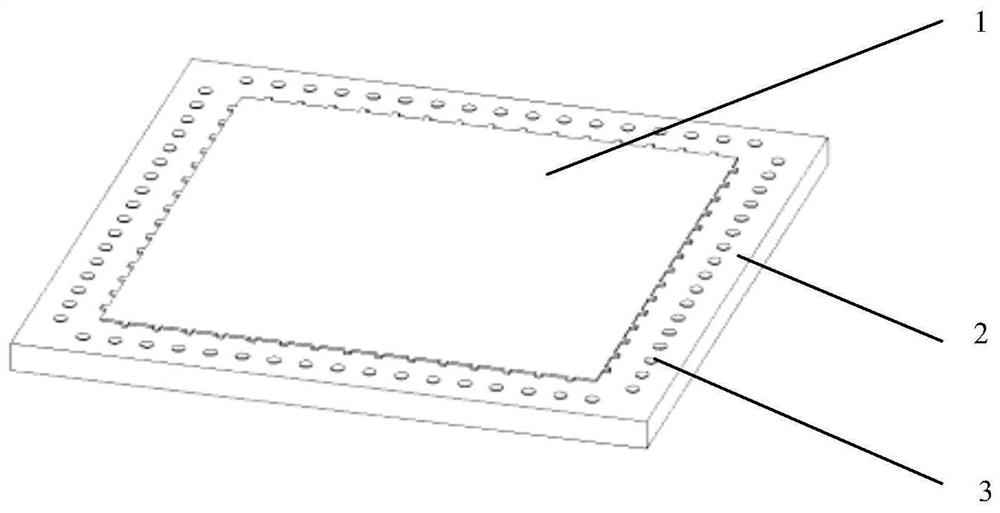
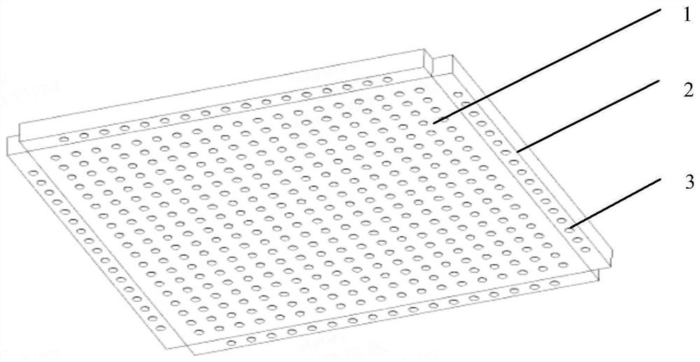
[0024] Please refer to figure 1 and figure 2 , this embodiment provides a chip pin expansion device, including:

[0025] Expansion boards 2 of various sizes and specifications are provided with a plurality of regularly arranged pins 3 on the expansion board 2 , and the arrangement distance of the pins 3 on the expansion board 2 is the same as that of the pins 3 on the main chip 1 . Therefore, the number of pins 3 on the expansion board 2 is determined by the size of the expansion board 2 .

[0026] The expansion board 2 is welded to the edge of the main chip 1 to expand the number of pins 3 of the main chip 1 . All four sides of the main chip 1 can be welded with the expansion board 2 .

[0027] If the expansion chip pin 3 is not used, there is an insulating protective mold around the pin 3 on the upper end of the chip to prevent the newly added pin 3 from being exposed.

[0028] BGA is to connect the chip pins to the PCB by soldering the solder balls on the bottom of the...


PUM


Abstract

The invention provides a chip pin expansion device which comprises an expansion board, a plurality of regularly arranged pins are arranged on the expansion board, the expansion board is welded to theedge of a main chip, and the number of the pins of the main chip is increased. According to the invention, the I/O quantity can be expanded in BGA packaging of the same size. By changing the structureof the chip and increasing the number of the pins, the function requirement is met, meanwhile, the occupied space of a PCB can be saved, the PCB design time is shortened, and the chip is suitable forapplication and popularization.

Description

technical field [0001] The invention belongs to the technical field of PCB, in particular to a chip pin expansion device. Background technique [0002] With the advancement of technology, the integration level of chips continues to increase, and the I / O pins increase sharply. In order to meet the needs of development, BGA packaging has begun to be widely used. BGA (Ball Grid Array) is a relatively common packaging form for chips at present, and BGA is a high-density surface mount packaging technology. On the bottom of the package, the pins are ball-shaped and arranged in a grid-like pattern, hence the name BGA. [0003] The number of I / Os of existing BGA packaged devices is mainly determined by the size of the package and the pitch of solder balls. Since the solder balls of the BGA package are arranged in an array under the package substrate, the number of I / Os of the device can be greatly increased, the package size can be reduced, and the assembly space can be saved. Th...

Claims


Application Information

Patent Timeline
IPC IPC(8): H05K1/18
CPCH05K1/181H05K2201/10
Inventor 司云
Owner SUZHOU LANGCHAO INTELLIGENT TECH CO LTD
Why Eureka
Try Eureka